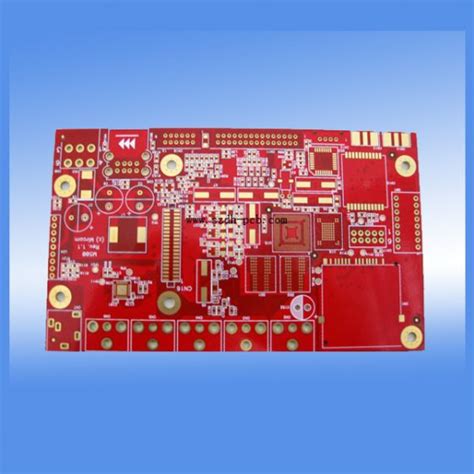
What are HDI PCBs?
HDI PCBs, also known as High Density Interconnector PCBs, are a type of printed circuit board that features a higher wiring density than traditional PCBs. They are characterized by their fine pitch traces, small vias, and high layer counts, enabling them to accommodate a large number of components in a compact space.
The primary features of HDI PCBs include:
– Fine pitch traces (usually less than 100 microns)
– Small vias (typically less than 150 microns in diameter)
– High layer counts (often 8 or more layers)
– Thin substrates (usually less than 1.6mm thick)
These features allow HDI PCBs to offer superior performance, reliability, and functionality compared to traditional PCBs.
Benefits of HDI PCBs
HDI PCBs offer several advantages over conventional PCBs, making them an attractive choice for many applications. Some of the key benefits of HDI PCBs include:
-
Miniaturization: The high wiring density of HDI PCBs allows for the creation of smaller, more compact devices, which is essential in today’s technology-driven world.
-
Improved signal integrity: The fine pitch traces and small vias in HDI PCBs reduce signal distortion and crosstalk, resulting in better signal integrity and overall performance.
-
Increased functionality: With the ability to accommodate more components in a smaller area, HDI PCBs enable the development of more complex and feature-rich devices.
-
Reduced weight: The thin substrates used in HDI PCBs contribute to lighter end products, which is particularly important in applications such as aerospace and portable electronics.
-
Cost-effectiveness: Although the initial manufacturing costs of HDI PCBs may be higher than traditional PCBs, their ability to incorporate more functionality into a smaller space often results in overall cost savings.

Applications of HDI PCBs
HDI PCBs find applications in a wide range of industries, particularly those that require high-performance, compact, and reliable electronic devices. Some of the most common applications of HDI PCBs include:
-
Smartphones and tablets: The demand for smaller, more powerful mobile devices has driven the adoption of HDI PCBs in the consumer electronics industry.
-
Wearable technology: Smartwatches, fitness trackers, and other wearable devices rely on HDI PCBs to achieve their compact size and advanced features.
-
Medical devices: HDI PCBs are used in various medical devices, such as implantable devices, monitoring systems, and diagnostic equipment, where reliability and miniaturization are crucial.
-
Aerospace and defense: The aerospace and defense industries employ HDI PCBs in applications that require high performance, reliability, and weight reduction, such as avionics, satellites, and military communications systems.
-
Automotive electronics: As vehicles become more technologically advanced, HDI PCBs are increasingly used in automotive applications, such as infotainment systems, driver assistance features, and electric vehicle components.

RAYPCB’s HDI PCB Manufacturing Process
RAYPCB employs state-of-the-art manufacturing processes and strict quality control measures to produce high-quality HDI PCBs. The company’s HDI PCB manufacturing process involves several key steps:
-
Design and Preparation: The process begins with the customer providing the PCB design files to RAYPCB. The company’s experienced engineers review the design for manufacturability and make any necessary adjustments to ensure optimal performance and reliability.
-
Material Selection: RAYPCB carefully selects the appropriate substrate material, copper foil, and other components based on the specific requirements of the project, such as the desired thickness, thermal properties, and electrical characteristics.
-
Lamination: The selected materials are laminated together using high pressure and temperature to create a solid, multilayer structure. This step is critical in ensuring the integrity and reliability of the final product.
-
Drilling and Plating: High-precision drilling machines create the small vias and holes required for HDI PCBs. The drilled holes are then plated with copper to establish electrical connections between layers.
-
Patterning: Using photolithography and etching techniques, the desired circuit patterns are transferred onto the copper layers. This process involves applying a photoresist coating, exposing it to UV light through a patterned mask, and then etching away the unwanted copper.
-
Solder Mask and Silkscreen: A solder mask is applied to the PCB to protect the copper traces from oxidation and prevent short circuits. The silkscreen layer is then added to provide labels, logos, and other markings on the PCB surface.
-
Surface Finish: RAYPCB offers a variety of surface finishes, such as ENIG (Electroless Nickel Immersion Gold), HASL (Hot Air Solder Leveling), and OSP (Organic Solderability Preservative), depending on the customer’s requirements and the intended application.
-
Electrical Testing and Quality Control: Each HDI PCB undergoes rigorous electrical testing and quality control inspections to ensure that it meets the specified performance and reliability standards. RAYPCB employs advanced testing equipment and follows strict quality control procedures to guarantee the highest level of product quality.
-
Packaging and Shipping: After passing all quality checks, the HDI PCBs are carefully packaged and shipped to the customer, with RAYPCB ensuring secure and timely delivery.

RAYPCB’s HDI PCB Specifications
RAYPCB offers a wide range of HDI PCB specifications to meet the diverse needs of its customers. Some of the key specifications are outlined in the table below:
| Parameter | Specification |
|---|---|
| Board Thickness | 0.4mm – 3.2mm |
| Layer Count | 4 – 24 layers |
| Minimum Trace Width/Spacing | 50μm/50μm |
| Minimum Via Diameter | 75μm |
| Minimum Via Pad Diameter | 250μm |
| Minimum Hole Size | 0.1mm |
| Aspect Ratio | 8:1 max |
| Surface Finish | ENIG, HASL, OSP, ImAg, ImSn |
| Solder Mask | Green, Red, Yellow, Blue, White, Black |
| Material | FR-4, Rogers, Polyimide, Teflon, Isola |
These specifications demonstrate RAYPCB’s capability to produce HDI PCBs with a high level of precision and customization, catering to a wide array of industries and applications.
Frequently Asked Questions (FAQ)
-
What is the minimum order quantity for HDI PCBs at RAYPCB?
RAYPCB offers flexible minimum order quantities for HDI PCBs, with the specific MOQ depending on the complexity and specifications of the project. For standard HDI PCBs, the MOQ can be as low as 5 pieces. However, for more complex designs or specific requirements, the MOQ may be higher. It is best to contact RAYPCB’s sales team to discuss your specific project needs and obtain a accurate MOQ. -
How long does it take for RAYPCB to manufacture HDI PCBs?
The lead time for HDI PCB manufacturing at RAYPCB depends on various factors, such as the complexity of the design, the required specifications, and the current production schedule. On average, the lead time for standard HDI PCBs ranges from 7 to 15 working days. However, for rush orders or more complex projects, the lead time may be longer. RAYPCB strives to provide the fastest possible turnaround time while maintaining the highest quality standards. -
What file formats does RAYPCB accept for HDI PCB design submission?
RAYPCB accepts a variety of file formats for HDI PCB design submission, including Gerber files (RS-274X), ODB++ files, and CAD files (such as Altium Designer, Cadence Allegro, and Mentor Graphics PADS). When submitting your design files, it is essential to ensure that all the necessary layers, drill files, and solder mask files are included. RAYPCB’s technical support team can assist you with any questions or concerns regarding file formats and design submission. -
Does RAYPCB offer assembly services for HDI PCBs?
Yes, RAYPCB offers a full range of assembly services for HDI PCBs, including SMT (Surface Mount Technology) and THT (Through-Hole Technology) assembly. The company has state-of-the-art assembly lines and a team of experienced professionals to ensure the highest quality assembly services. RAYPCB can assist with component sourcing, testing, and final product packaging, providing a one-stop solution for your HDI PCB needs. -
How does RAYPCB ensure the quality of its HDI PCBs?
RAYPCB employs a comprehensive quality control system to ensure the highest quality of its HDI PCBs. This includes strict adherence to industry standards, such as IPC-A-600, IPC-6012, and ISO 9001:2015. The company uses advanced testing equipment, such as flying probe testers, automated optical inspection (AOI) machines, and X-ray inspection systems, to detect any defects or anomalies in the PCBs. Additionally, RAYPCB has a dedicated quality control team that oversees the entire manufacturing process, from material selection to final inspection, ensuring that each HDI PCB meets the specified requirements and performance standards.
Conclusion
HDI PCBs have revolutionized the electronics industry, enabling the development of smaller, more powerful, and more reliable devices. RAYPCB, with its state-of-the-art manufacturing facilities, experienced team, and commitment to quality, is a leading provider of HDI PCBs for a wide range of industries and applications.
By understanding the features, benefits, and applications of HDI PCBs, as well as RAYPCB’s manufacturing process and specifications, customers can make informed decisions when selecting a PCB manufacturer for their projects. With RAYPCB’s expertise and support, customers can bring their innovative ideas to life, pushing the boundaries of what is possible in the world of electronics.
Leave a Reply