Table of Contents
- Introduction to ViaInPad
- Advantages of Using ViaInPad
- Space Savings
- Improved Signal Integrity
- Reduced Layer Count
- Enhanced Thermal Performance
- Limitations and Challenges of ViaInPad
- Manufacturing Complexity
- Increased Cost
- Reduced Solder Joint Reliability
- Potential for Solder Wicking
- Design Considerations for ViaInPad
- Via Size and Pad Size
- Via Placement
- Solder Mask Design
- Thermal Relief Patterns
- Manufacturing Process for ViaInPad
- Via Filling
- Solder Mask Application
- Surface Finish Selection
- Applications of ViaInPad
- High-Density Interconnect (HDI) PCBs
- RF and Microwave PCBs
- Automotive and Aerospace Electronics
- Alternative Techniques to ViaInPad
- Blind and Buried Vias
- Microvias
- Via Tenting
- Best Practices for Implementing ViaInPad
- Frequently Asked Questions (FAQ)
- Conclusion
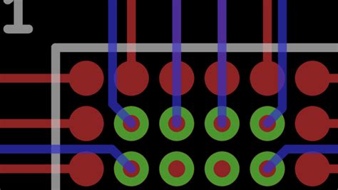
Introduction to ViaInPad
ViaInPad is a PCB design technique that involves placing vias directly on the surface mount pads of components, as opposed to the traditional approach of placing vias adjacent to the pads. This technique has gained traction in recent years due to its ability to save space, improve signal integrity, and enhance thermal performance.
In a conventional PCB design, vias are typically placed near the component pads, requiring additional space on the board. By placing the vias directly on the pads, designers can reduce the overall footprint of the component and free up valuable board space for other components or routing.

Advantages of Using ViaInPad
Space Savings
One of the primary advantages of using ViaInPad is the significant space savings it offers. By placing vias directly on the component pads, designers can reduce the overall footprint of the component, allowing for more compact PCB designs. This is particularly beneficial in applications where board space is limited, such as wearable devices, smartphones, and IoT sensors.
Improved Signal Integrity
ViaInPad can also improve signal integrity by reducing the length of the signal path between the component and the via. In traditional designs, the signal must travel from the component pad to the via, which can introduce unwanted inductance and capacitance. By placing the via directly on the pad, the signal path is minimized, reducing the potential for signal distortion and improving overall signal quality.
Reduced Layer Count
Another advantage of ViaInPad is the potential for reducing the number of layers in a PCB. By placing vias on the component pads, designers can often eliminate the need for additional routing layers, as the vias can provide direct connections between layers. This can lead to simpler, more cost-effective PCB designs.
Enhanced Thermal Performance
ViaInPad can also improve the thermal performance of a PCB by providing a direct thermal path from the component to the inner layers of the board. This is particularly beneficial for components that generate significant heat, such as power MOSFETs and high-performance processors. By placing vias on the pads, designers can effectively transfer heat away from the component, improving reliability and longevity.

Limitations and Challenges of ViaInPad
While ViaInPad offers numerous benefits, it also presents some limitations and challenges that designers must consider.
Manufacturing Complexity
One of the primary challenges of ViaInPad is the increased manufacturing complexity compared to traditional PCB designs. Placing vias directly on the component pads requires precise alignment and drilling, which can be more difficult to achieve than placing vias adjacent to the pads. This can lead to higher manufacturing costs and longer production times.
Increased Cost
The increased manufacturing complexity of ViaInPad can also result in higher costs compared to traditional PCB designs. The precise alignment and drilling required for ViaInPad may necessitate specialized equipment and skilled labor, which can drive up production costs. Additionally, the need for via filling and other specialized processes can further increase the overall cost of the PCB.
Reduced Solder Joint Reliability
Another potential limitation of ViaInPad is the reduced solder joint reliability compared to traditional designs. When vias are placed directly on the component pads, the solder joint must accommodate both the component lead and the via, which can result in a smaller and potentially weaker solder joint. This can lead to increased stress on the joint during thermal cycling and vibration, potentially reducing the overall reliability of the solder connection.
Potential for Solder Wicking
ViaInPad designs also present the potential for solder wicking, where solder can flow into the via during the soldering process. This can lead to insufficient solder on the component pad, resulting in a weak or unreliable solder joint. To mitigate this issue, designers must carefully consider the size and placement of the vias, as well as the solder mask design.

Design Considerations for ViaInPad
When implementing ViaInPad in a PCB design, there are several key considerations that designers must take into account to ensure optimal performance and reliability.
Via Size and Pad Size
The size of the via and the component pad are critical factors in ViaInPad design. The via must be small enough to fit within the pad without compromising the solder joint, but large enough to provide adequate electrical and thermal conductivity. Designers must also ensure that the pad size is sufficient to accommodate both the component lead and the via.
Via Placement
The placement of the via on the component pad is another important consideration. Vias should be placed as close to the center of the pad as possible to minimize the potential for solder wicking and ensure a reliable solder joint. However, designers must also consider the placement of the via in relation to the component lead to avoid any potential interference or shorting.
Solder Mask Design
The solder mask design is crucial in ViaInPad to prevent solder wicking and ensure a reliable solder joint. Designers must carefully control the solder mask opening around the via to provide adequate clearance for the solder while still preventing solder from flowing into the via. This may require the use of specialized solder mask designs, such as via tenting or solder mask plugging.
Thermal Relief Patterns
Thermal relief patterns are another important consideration in ViaInPad design, particularly for components that generate significant heat. These patterns typically consist of spokes or webs that connect the via to the surrounding copper, providing a path for heat to dissipate while minimizing the potential for solder wicking. Designers must carefully balance the thermal relief pattern with the electrical requirements of the component to ensure optimal performance.
Manufacturing Process for ViaInPad
The manufacturing process for ViaInPad involves several specialized steps beyond those required for traditional PCB designs.
Via Filling
One of the key steps in ViaInPad manufacturing is via filling, where the vias are filled with a conductive material to prevent solder wicking and provide a smooth surface for component placement. There are several methods for via filling, including:
- Conductive epoxy filling
- Electroplating
- Screen printing
- Conductive paste filling
The choice of via filling method depends on the specific requirements of the design, such as the desired electrical and thermal conductivity, the cost, and the manufacturing capabilities of the PCB fabricator.
Solder Mask Application
Another critical step in ViaInPad manufacturing is the application of the solder mask. As mentioned earlier, the solder mask design is crucial in preventing solder wicking and ensuring a reliable solder joint. PCB fabricators must use specialized equipment and techniques to apply the solder mask accurately and consistently around the vias.
Surface Finish Selection
The choice of surface finish is also important in ViaInPad manufacturing, as it can impact the solderability and reliability of the solder joint. Some common surface finishes used in ViaInPad include:
- Immersion silver (IAg)
- Electroless nickel immersion gold (ENIG)
- Organic solderability preservative (OSP)
The selection of the surface finish depends on factors such as the desired shelf life, the soldering process, and the environmental conditions the PCB will be exposed to.
Applications of ViaInPad
ViaInPad is particularly well-suited for certain applications where space savings, signal integrity, and thermal performance are critical.
High-Density Interconnect (HDI) PCBs
HDI PCBs are characterized by their high component density and fine pitch features. ViaInPad is often used in HDI designs to maximize space utilization and provide direct connections between layers. This can enable the design of highly compact and complex PCBs for applications such as smartphones, tablets, and wearable devices.
RF and Microwave PCBs
ViaInPad is also commonly used in RF and microwave PCBs, where signal integrity and controlled impedance are critical. By placing vias directly on the component pads, designers can minimize the signal path length and reduce the potential for signal distortion. This can help to ensure optimal performance in high-frequency applications such as 5G networks, radar systems, and satellite communications.
Automotive and Aerospace Electronics
ViaInPad is also finding increasing use in automotive and aerospace electronics, where reliability and thermal performance are paramount. By providing a direct thermal path from the component to the inner layers of the board, ViaInPad can help to dissipate heat more effectively and improve the overall reliability of the system. This is particularly important in harsh environments where high temperatures and vibration are common.
Alternative Techniques to ViaInPad
While ViaInPad offers many benefits, it is not always the best choice for every PCB design. There are several alternative techniques that designers can consider, depending on the specific requirements of the application.
Blind and Buried Vias
Blind and buried vias are another space-saving technique that can be used in PCB design. Blind vias are drilled from one surface of the board to an inner layer, while buried vias are drilled between inner layers and do not extend to either surface. These vias can provide direct connections between layers without consuming space on the surface of the board.
Microvias
Microvias are small-diameter vias that are typically less than 150 microns in diameter. They can be used to provide high-density interconnects between layers and are often used in HDI designs. Microvias can be stacked or staggered to create complex routing patterns and can be filled with conductive material to improve thermal performance.
Via Tenting
Via tenting is a technique where the via is covered with solder mask on one or both sides of the board. This can help to prevent solder wicking and improve the reliability of the solder joint. Via tenting is often used in conjunction with ViaInPad to provide additional protection against solder wicking.
Best Practices for Implementing ViaInPad
To ensure the success of a ViaInPad design, there are several best practices that designers should follow:
- Work closely with the PCB fabricator to ensure that they have the necessary capabilities and experience to manufacture ViaInPad designs.
- Use simulation tools to optimize the placement and size of the vias and ensure that they meet the electrical and thermal requirements of the design.
- Follow the recommended design guidelines for via size, pad size, and solder mask design to ensure optimal performance and reliability.
- Use filled vias whenever possible to improve thermal conductivity and prevent solder wicking.
- Consider the use of thermal relief patterns to improve heat dissipation and minimize the potential for solder wicking.
- Test the design thoroughly to ensure that it meets the required performance and reliability standards.
Frequently Asked Questions (FAQ)
-
What is the minimum via size that can be used in ViaInPad?
The minimum via size depends on the capabilities of the PCB fabricator, but is typically around 0.2mm to 0.3mm in diameter. -
Can ViaInPad be used with BGA components?
Yes, ViaInPad can be used with BGA components, but it requires careful design and precise alignment to ensure that the vias do not interfere with the solder balls. -
Is ViaInPad more expensive than traditional PCB designs?
Yes, ViaInPad can be more expensive than traditional designs due to the increased manufacturing complexity and the need for specialized processes such as via filling and solder mask application. -
Can ViaInPad be used in high-voltage applications?
ViaInPad can be used in high-voltage applications, but designers must carefully consider the voltage rating of the vias and ensure that they are adequately isolated to prevent arcing and other issues. -
What is the main benefit of using filled vias in ViaInPad?
The main benefit of using filled vias in ViaInPad is improved thermal conductivity and the prevention of solder wicking. Filled vias provide a solid connection between the component pad and the inner layers of the board, allowing heat to dissipate more effectively and preventing solder from flowing into the via during the soldering process.
Conclusion
ViaInPad is a powerful PCB design technique that offers significant benefits in terms of space savings, signal integrity, and thermal performance. By placing vias directly on the component pads, designers can create highly compact and efficient PCBs that are well-suited for a wide range of applications, from high-density interconnects to automotive and aerospace electronics.
However, ViaInPad also presents some challenges and limitations, including increased manufacturing complexity, higher costs, and the potential for reduced solder joint reliability. Designers must carefully consider these factors and follow best practices to ensure the success of their ViaInPad designs.
As PCB technology continues to evolve, it is likely that ViaInPad will become an increasingly important tool in the designer’s toolkit. By understanding the benefits and limitations of this technique and applying it appropriately, designers can create PCBs that push the boundaries of performance and functionality.
Leave a Reply