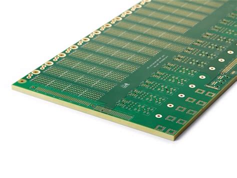
Introduction to Copper-Based Printed Circuit Boards
Printed Circuit Boards (PCBs) are the backbone of modern electronics. They provide a platform for electronic components to be mounted and interconnected, forming a complete circuit. Among the various types of PCBs, copper-based PCBs are the most widely used due to their excellent electrical conductivity, thermal stability, and cost-effectiveness. In this article, we will delve into the world of copper-based PCBs, exploring their manufacturing process, advantages, applications, and more.
The Role of Copper in PCBs
Copper is a vital material in the production of PCBs due to its outstanding electrical and thermal properties. Some of the key reasons why copper is used in PCBs include:
- High electrical conductivity: Copper has one of the highest electrical conductivities among metals, allowing for efficient transfer of electrical signals.
- Thermal stability: Copper’s excellent thermal conductivity helps dissipate heat generated by electronic components, preventing overheating and ensuring stable performance.
- Cost-effectiveness: Compared to other highly conductive metals like silver or gold, copper is relatively inexpensive, making it an economical choice for PCB manufacturing.
Copper Thickness in PCBs
The thickness of the copper layer in a PCB is measured in ounces per square foot (oz/ft²). The most common copper thicknesses used in PCBs are:
| Copper Weight (oz/ft²) | Thickness (μm) | Typical Applications |
|---|---|---|
| 0.5 oz | 17.5 | Low-power, high-density designs |
| 1 oz | 35 | Most common, general-purpose |
| 2 oz | 70 | High-current, power electronics |
| 3 oz | 105 | Heavy-duty, high-power applications |
Choosing the appropriate copper thickness depends on the specific requirements of the electronic device, such as current carrying capacity, heat dissipation, and mechanical strength.

Manufacturing Process of Copper-Based PCBs
The manufacturing process of copper-based PCBs involves several steps, each requiring precision and accuracy to ensure the final product meets the desired specifications. The main steps in the process are:
1. Substrate Preparation
The PCB substrate, typically made of fiberglass-reinforced epoxy (FR-4), is cut to the required size and shape. The substrate is then cleaned to remove any contaminants that may affect the adhesion of the copper layer.
2. Copper Cladding
A thin layer of copper is laminated onto the substrate using heat and pressure. The copper-clad substrate is then allowed to cool and stabilize.
3. Drilling
Holes are drilled into the PCB to accommodate through-hole components and provide interconnections between layers. The drilling process is usually done using computer-controlled drill machines for precision and accuracy.
4. Patterning
The desired circuit pattern is transferred onto the copper layer using a photolithographic process. This involves applying a light-sensitive photoresist coating, exposing it to UV light through a photomask, and developing the resist to reveal the circuit pattern.
5. Etching
The exposed copper areas are chemically etched away, leaving behind the desired circuit pattern. The remaining photoresist is then removed, revealing the final copper traces.
6. Plating
Additional copper plating may be applied to the traces to increase their thickness and improve their current carrying capacity. Other finishes, such as solder mask and silkscreen, are also applied to protect the PCB and provide labeling for components.
7. Surface Finish
A surface finish, such as HASL (Hot Air Solder Leveling), ENIG (Electroless Nickel Immersion Gold), or OSP (Organic Solderability Preservative), is applied to the exposed copper areas to prevent oxidation and enhance solderability.

Advantages of Copper-Based PCBs
Copper-based PCBs offer several advantages over other types of PCBs, making them the preferred choice for a wide range of applications. Some of the key advantages include:
-
Excellent electrical conductivity: Copper’s high electrical conductivity ensures efficient signal transfer and minimal losses, resulting in better performance and reliability.
-
Thermal stability: Copper’s thermal conductivity helps dissipate heat generated by electronic components, preventing overheating and ensuring stable operation.
-
Cost-effectiveness: Copper is relatively inexpensive compared to other highly conductive metals, making copper-based PCBs an economical choice for electronic devices.
-
Versatility: Copper-based PCBs can be manufactured in various thicknesses, sizes, and shapes, making them suitable for a wide range of applications, from small consumer electronics to large industrial systems.
-
Durability: With proper design and manufacturing, copper-based PCBs can withstand harsh environmental conditions, mechanical stress, and repeated thermal cycles, ensuring long-term reliability.

Applications of Copper-Based PCBs
Copper-based PCBs find applications in virtually every sector of the electronics industry. Some of the most common applications include:
-
Consumer electronics: Smartphones, laptops, tablets, televisions, and home appliances.
-
Automotive electronics: Engine control units, infotainment systems, sensors, and safety systems.
-
Industrial electronics: Process control systems, automation equipment, power electronics, and instrumentation.
-
Medical devices: Diagnostic equipment, monitoring systems, and implantable devices.
-
Aerospace and defense: Avionics, communication systems, radar, and satellite equipment.
-
Internet of Things (IoT): Smart home devices, wearables, and sensor networks.
The widespread use of copper-based PCBs across various industries is a testament to their reliability, performance, and cost-effectiveness.
Copper-Based PCB Design Considerations
When designing a copper-based PCB, several factors must be considered to ensure optimal performance, reliability, and manufacturability. Some of the key design considerations include:
1. Trace Width and Spacing
The width of the copper traces and the spacing between them must be carefully designed to ensure proper signal integrity, current carrying capacity, and manufacturability. Factors such as the operating frequency, current requirements, and PCB thickness must be taken into account when determining trace width and spacing.
2. Via Design
Vias are used to interconnect different layers of a multi-layer PCB. The size, placement, and type of vias (through-hole, blind, or buried) must be optimized to minimize signal reflections, crosstalk, and manufacturing challenges.
3. Impedance Control
For high-speed digital and RF circuits, maintaining proper impedance control is crucial for signal integrity. This involves designing the PCB Stack-Up, trace geometry, and dielectric materials to achieve the desired characteristic impedance.
4. Thermal Management
Proper thermal management is essential to prevent overheating and ensure reliable operation. This can be achieved through the use of thermal vias, copper pours, and heat sinks, as well as optimizing component placement and airflow.
5. EMI/EMC Considerations
Electromagnetic Interference (EMI) and Electromagnetic Compatibility (EMC) must be considered to ensure the PCB does not interfere with other electronic devices and meets regulatory requirements. This can be achieved through proper grounding, shielding, and filtering techniques.
Future Trends in Copper-Based PCBs
As electronic devices continue to evolve, so do the requirements for PCBs. Some of the emerging trends in copper-based PCBs include:
-
High-Density Interconnect (HDI): HDI PCBs feature smaller trace widths, tighter spacing, and micro-vias, enabling the integration of more components in a smaller footprint.
-
Flexible and Rigid-flex PCBs: Flexible and rigid-flex PCBs offer increased design freedom, allowing for the creation of three-dimensional electronic assemblies and wearable devices.
-
Embedded Components: Embedding active and passive components within the PCB substrate can save space, reduce parasitic effects, and improve overall system performance.
-
Advanced Materials: New substrate materials, such as low-loss dielectrics and high-temperature laminates, are being developed to meet the demands of high-speed and harsh-environment applications.
-
Additive Manufacturing: 3D printing techniques, such as inkjet printing and aerosol jet printing, are being explored for the fabrication of copper-based PCBs, offering the potential for rapid prototyping and customization.
FAQ
1. What is the difference between copper-based PCBs and other types of PCBs?
Copper-based PCBs use copper as the primary conductive material for the traces and pads, while other types of PCBs may use different materials, such as aluminum or conductive inks. Copper is preferred due to its high electrical conductivity, thermal stability, and cost-effectiveness.
2. Can copper-based PCBs be used for high-frequency applications?
Yes, copper-based PCBs can be used for high-frequency applications, such as RF and microwave circuits. However, proper design considerations, such as impedance control, signal integrity, and EMI/EMC, must be taken into account to ensure optimal performance.
3. How does the thickness of the copper layer affect PCB performance?
The thickness of the copper layer, measured in ounces per square foot (oz/ft²), affects the current carrying capacity, heat dissipation, and mechanical strength of the PCB. Thicker copper layers can handle higher currents and provide better thermal management, but may increase the overall cost and weight of the PCB.
4. What surface finishes are commonly used for copper-based PCBs?
Common surface finishes for copper-based PCBs include HASL (Hot Air Solder Leveling), ENIG (Electroless Nickel Immersion Gold), and OSP (Organic Solderability Preservative). The choice of surface finish depends on factors such as solderability, shelf life, cost, and compatibility with the assembly process.
5. Are copper-based PCBs environmentally friendly?
Copper-based PCBs can be made more environmentally friendly by using lead-free solder, halogen-free materials, and implementing proper recycling and disposal practices. Many PCB manufacturers now offer eco-friendly options that comply with RoHS (Restriction of Hazardous Substances) and WEEE (Waste Electrical and Electronic Equipment) directives.
Conclusion
Copper-based PCBs are the backbone of modern electronics, offering excellent electrical conductivity, thermal stability, and cost-effectiveness. Their versatility and reliability make them suitable for a wide range of applications, from consumer electronics to aerospace and defense. As electronic devices continue to advance, copper-based PCBs are evolving to meet the ever-increasing demands for performance, functionality, and sustainability. By understanding the manufacturing process, design considerations, and future trends in copper-based PCBs, engineers and designers can create innovative and reliable electronic products that shape our world.
Leave a Reply