Introduction to PCB Inductance
Printed Circuit Board (PCB) inductance is a crucial factor in the design and performance of high-speed electronic circuits. Inductance is the property of a conductor that opposes changes in current flow, resulting in the storage of magnetic energy. In PCBs, traces act as inductors, and their inductance can significantly impact signal integrity, power integrity, and electromagnetic compatibility (EMC) of the circuit.
Understanding and accurately calculating the inductance of PCB traces is essential for designers to optimize circuit performance, minimize signal distortion, and ensure reliable operation. This article will provide a comprehensive guide on how to calculate the inductance of PCB traces, covering the fundamentals of inductance, factors affecting PCB trace inductance, calculation methods, and practical examples.
Fundamentals of Inductance
What is Inductance?
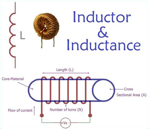
Inductance is an electrical property that describes the ability of a conductor to store magnetic energy when an electric current flows through it. It is measured in henries (H) and is represented by the symbol “L.” Inductance is defined as the ratio of the magnetic flux linkage to the current flowing through the conductor.
L = Φ / I
Where:
– L is the inductance in henries (H)
– Φ is the magnetic flux linkage in webers (Wb)
– I is the current in amperes (A)
Self-Inductance and Mutual Inductance
There are two types of inductance: self-inductance and mutual inductance.
-
Self-Inductance: Self-inductance is the property of a conductor that opposes changes in the current flowing through it, resulting in the storage of magnetic energy in the conductor itself. It is the inductance of a single conductor and is determined by its geometry and material properties.
-
Mutual Inductance: Mutual inductance is the property of two or more conductors that are magnetically coupled, where a change in current in one conductor induces a voltage in the other conductor(s). Mutual inductance depends on the geometry and spacing of the conductors, as well as their material properties.
Factors Affecting Inductance
Several factors influence the inductance of a conductor, including:
-
Conductor geometry: The shape, length, and cross-sectional area of the conductor affect its inductance. Longer and thinner conductors have higher inductance than shorter and thicker conductors.
-
Magnetic permeability: The magnetic permeability of the conductor material and the surrounding medium affects the inductance. Materials with higher magnetic permeability, such as ferromagnetic materials, have higher inductance than materials with lower magnetic permeability, such as air or vacuum.
-
Frequency: The inductance of a conductor can vary with the frequency of the current flowing through it. At high frequencies, skin effect and proximity effect can change the effective inductance of the conductor.
-
Proximity to other conductors: The presence of other conductors near the conductor of interest can influence its inductance through mutual inductance effects.

Factors Affecting PCB Trace Inductance
PCB trace inductance is influenced by several factors, including trace geometry, trace spacing, substrate properties, and the presence of nearby conductors. Understanding these factors is crucial for accurate inductance calculation and PCB Design optimization.
Trace Geometry
The geometry of a PCB trace, including its length, width, and thickness, has a significant impact on its inductance. The inductance of a straight trace can be approximated using the following formula:
L = 0.002 × l × [ln(2l / (w + t)) + 0.5 + 0.2235 × (w + t) / l] (nH)
Where:
– L is the inductance in nanohenries (nH)
– l is the length of the trace in centimeters (cm)
– w is the width of the trace in centimeters (cm)
– t is the thickness of the trace in centimeters (cm)
From this formula, it is evident that longer and thinner traces have higher inductance than shorter and wider traces.
Trace Spacing
The spacing between PCB traces affects their mutual inductance. Traces that are closer together have higher mutual inductance than traces that are farther apart. The mutual inductance between two parallel traces can be approximated using the following formula:
M = 0.002 × l × [ln(2l / d) – 1 + d / l] (nH)
Where:
– M is the mutual inductance in nanohenries (nH)
– l is the length of the traces in centimeters (cm)
– d is the center-to-center spacing between the traces in centimeters (cm)
To minimize mutual inductance, designers should ensure adequate spacing between traces, especially for high-speed signals or sensitive analog circuits.
Substrate Properties
The properties of the PCB substrate, such as its dielectric constant and thickness, can affect the inductance of the traces. The dielectric constant of the substrate material determines the velocity of propagation of signals along the traces, which in turn affects the inductance. The inductance of a trace on a PCB substrate can be approximated using the following formula:
L = 0.002 × l × [ln(2h / w) + 0.5 + 0.2235 × w / h] (nH)
Where:
– L is the inductance in nanohenries (nH)
– l is the length of the trace in centimeters (cm)
– w is the width of the trace in centimeters (cm)
– h is the height of the trace above the ground plane in centimeters (cm)
Thicker substrates and higher dielectric constants result in lower trace inductance, while thinner substrates and lower dielectric constants lead to higher trace inductance.
Presence of Nearby Conductors
The presence of nearby conductors, such as ground planes, power planes, or other traces, can influence the inductance of a PCB trace through mutual inductance effects. Ground planes and power planes can provide a low-impedance return path for high-frequency currents, effectively reducing the inductance of the traces. On the other hand, nearby traces can increase the mutual inductance, leading to signal coupling and potential signal integrity issues.
To minimize the impact of nearby conductors on trace inductance, designers should:
- Use ground planes and power planes to provide low-impedance return paths
- Ensure adequate spacing between traces to minimize mutual inductance
- Use guard traces or shielding to isolate sensitive signals from interfering conductors

Calculation Methods for PCB Trace Inductance
There are several methods for calculating the inductance of PCB traces, ranging from simple approximations to more accurate numerical simulations. The choice of the calculation method depends on the required accuracy, the complexity of the PCB Layout, and the available resources.
Analytical Formulas
Analytical formulas, such as the ones presented in the previous sections, provide quick and easy approximations of PCB trace inductance. These formulas are based on simplified geometric models and assume ideal conditions, such as uniform trace cross-sections and homogeneous dielectric materials. While analytical formulas are useful for rough estimates and initial design decisions, they may not account for all the factors affecting trace inductance in real-world PCB layouts.
Numerical Simulations
Numerical simulations, such as finite element analysis (FEA) or method of moments (MoM), offer more accurate and comprehensive calculations of PCB trace inductance. These methods discretize the PCB layout into small elements and solve Maxwell’s equations to determine the electromagnetic fields and inductances associated with each element. Numerical simulations can account for complex trace geometries, non-uniform cross-sections, and inhomogeneous dielectric materials, providing more realistic results than analytical formulas.
However, numerical simulations require specialized software tools and can be time-consuming and computationally intensive, especially for large and complex PCB layouts. Designers should consider the trade-off between accuracy and computational cost when deciding on the appropriate calculation method.
Empirical Measurements
Empirical measurements involve directly measuring the inductance of PCB traces using specialized equipment, such as a vector network analyzer (VNA) or an impedance analyzer. These measurements provide the most accurate results, as they account for all the real-world factors affecting trace inductance, including manufacturing tolerances and material properties.
However, empirical measurements require physical prototypes and dedicated measurement setups, which can be costly and time-consuming. They are typically used for final verification and validation of PCB designs, rather than for initial design and optimization.

Practical Examples and Case Studies
To illustrate the application of PCB trace inductance calculation methods, we will present several practical examples and case studies.
Example 1: Calculating the Inductance of a Straight Trace
Consider a straight PCB trace with the following properties:
– Length (l) = 5 cm
– Width (w) = 0.2 cm
– Thickness (t) = 0.0035 cm
Using the analytical formula for the inductance of a straight trace:
L = 0.002 × l × [ln(2l / (w + t)) + 0.5 + 0.2235 × (w + t) / l] (nH)
Plugging in the values:
L = 0.002 × 5 × [ln(2 × 5 / (0.2 + 0.0035)) + 0.5 + 0.2235 × (0.2 + 0.0035) / 5] (nH)
L ≈ 7.6 nH
This example demonstrates how to use the analytical formula to quickly estimate the inductance of a simple straight trace.
Example 2: Calculating the Mutual Inductance between Two Parallel Traces
Consider two parallel PCB traces with the following properties:
– Length (l) = 10 cm
– Center-to-center spacing (d) = 0.5 cm
Using the analytical formula for the mutual inductance between two parallel traces:
M = 0.002 × l × [ln(2l / d) – 1 + d / l] (nH)
Plugging in the values:
M = 0.002 × 10 × [ln(2 × 10 / 0.5) – 1 + 0.5 / 10] (nH)
M ≈ 6.1 nH
This example shows how to estimate the mutual inductance between two parallel traces, which can be useful for assessing potential signal coupling and crosstalk.
Case Study: High-Speed Digital PCB Design
In this case study, we will consider the design of a high-speed digital PCB with the following requirements:
– Signal frequency: 1 GHz
– Maximum allowable inductance per trace: 5 nH
– PCB substrate: FR-4 with a dielectric constant (ε_r) of 4.4 and a thickness (h) of 0.16 cm
To meet the inductance requirement, we can use the analytical formula for the inductance of a trace on a PCB substrate to determine the maximum trace length:
L = 0.002 × l × [ln(2h / w) + 0.5 + 0.2235 × w / h] (nH)
Assuming a trace width (w) of 0.02 cm and solving for the maximum trace length (l_max):
5 = 0.002 × l_max × [ln(2 × 0.16 / 0.02) + 0.5 + 0.2235 × 0.02 / 0.16]
l_max ≈ 12.8 cm
To minimize mutual inductance between traces, we can use the analytical formula for the mutual inductance to determine the minimum trace spacing (d_min):
M = 0.002 × l × [ln(2l / d) – 1 + d / l] (nH)
Assuming a maximum allowable mutual inductance (M_max) of 1 nH and solving for the minimum trace spacing (d_min):
1 = 0.002 × 12.8 × [ln(2 × 12.8 / d_min) – 1 + d_min / 12.8]
d_min ≈ 0.8 cm
This case study demonstrates how to use analytical formulas to make initial design decisions for a high-speed digital PCB, considering both self-inductance and mutual inductance of the traces.
Conclusion
Calculating the inductance of PCB traces is essential for designing high-performance electronic circuits. By understanding the factors affecting PCB trace inductance and applying appropriate calculation methods, designers can optimize signal integrity, power integrity, and EMC of their PCB layouts.
This article has provided a comprehensive guide on how to calculate the inductance of PCB traces, covering the fundamentals of inductance, factors affecting PCB trace inductance, calculation methods, and practical examples. Designers should consider the trade-offs between accuracy, computational cost, and resource availability when choosing the most suitable calculation method for their specific design requirements.
By mastering the techniques for calculating PCB trace inductance, designers can create more reliable, efficient, and high-performance electronic systems.
Frequently Asked Questions (FAQ)
1. What is the difference between self-inductance and mutual inductance?
Self-inductance is the property of a single conductor that opposes changes in the current flowing through it, resulting in the storage of magnetic energy in the conductor itself. Mutual inductance, on the other hand, is the property of two or more conductors that are magnetically coupled, where a change in current in one conductor induces a voltage in the other conductor(s).
2. How does trace geometry affect PCB trace inductance?
Trace geometry, including length, width, and thickness, has a significant impact on PCB trace inductance. Longer and thinner traces have higher inductance than shorter and wider traces. This relationship is described by the analytical formula for the inductance of a straight trace:
L = 0.002 × l × [ln(2l / (w + t)) + 0.5 + 0.2235 × (w + t) / l] (nH)
Where L is the inductance, l is the length, w is the width, and t is the thickness of the trace.
3. What are the main factors influencing mutual inductance between PCB traces?
The main factors influencing mutual inductance between PCB traces are trace spacing and trace length. Traces that are closer together have higher mutual inductance than traces that are farther apart. The mutual inductance between two parallel traces can be approximated using the following formula:
M = 0.002 × l × [ln(2l / d) – 1 + d / l] (nH)
Where M is the mutual inductance, l is the length of the traces, and d is the center-to-center spacing between the traces.
4. How can PCB designers minimize the impact of trace inductance on signal integrity?
PCB designers can minimize the impact of trace inductance on signal integrity by:
- Keeping trace lengths as short as possible
- Using wider traces to reduce self-inductance
- Ensuring adequate spacing between traces to minimize mutual inductance
- Using ground planes and power planes to provide low-impedance return paths
- Employing guard traces or shielding to isolate sensitive signals from interfering conductors
5. What are the advantages and disadvantages of using numerical simulations for calculating PCB trace inductance?
Advantages of using numerical simulations for calculating PCB trace inductance include:
1. Higher accuracy compared to analytical formulas, as they can account for complex trace geometries, non-uniform cross-sections, and inhomogeneous dielectric materials
2. Ability to analyze complex PCB layouts and provide comprehensive results
Disadvantages of using numerical simulations include:
1. Requirement for specialized software tools, which can be expensive
2. Time-consuming and computationally intensive, especially for large and complex PCB layouts
3. Need for expertise in setting up and interpreting simulation results
Designers should consider the trade-off between accuracy and computational cost when deciding on the appropriate calculation method for their specific design requirements.
Leave a Reply