Introduction to High Current PCB Design
Printed circuit boards (PCBs) that carry high currents require special design considerations to ensure reliable operation and prevent issues such as overheating, voltage drop, and electromagnetic interference (EMI). High current PCBs are used in a variety of applications including power supplies, motor controllers, automotive electronics, and industrial equipment.
Challenges of High Current PCB Design
Designing PCBs for high current applications presents several challenges:
– Heat generation and thermal management
– Voltage drop across traces
– EMI and electromagnetic compatibility (EMC)
– Safety and reliability requirements
– Manufacturing limitations
Careful component selection, layout techniques, and analysis are needed to overcome these challenges and create robust high current PCB designs.
Key Considerations for High Current PCB Design
Current Carrying Capacity
The first step in designing a high current PCB is determining the required current carrying capacity of the traces. This depends on factors such as:
– Maximum current draw of components
– Ambient temperature
– Trace width, thickness, and length
– Number of copper layers
– Thermal reliefs and vias
The following table provides a rough guide to the current carrying capacity of copper traces based on their width and thickness:
| Trace Width (mm) | 1 oz Cu (0.035 mm) | 2 oz Cu (0.070 mm) |
|---|---|---|
| 0.25 | 0.5 A | 0.7 A |
| 0.50 | 1.0 A | 1.4 A |
| 1.00 | 2.0 A | 2.8 A |
| 2.00 | 4.0 A | 5.6 A |
| 4.00 | 8.0 A | 11.2 A |
For high current designs, using thicker copper, wider traces, and multiple layers is often necessary to achieve the required current capacity without excessive heating.
Trace Routing and Placement
Proper component placement and trace routing is critical in high current PCB design to minimize trace lengths, voltage drop, and loop areas that can cause EMI.
Some tips for optimizing high current trace routing include:
– Place high current components close together
– Use wide, short traces
– Provide solid copper pours for power and ground
– Route power traces on inner layers when possible
– Avoid sharp corners and use 45° routing
– Keep sensitive signals away from high current traces
– Use ground planes and shields to reduce EMI
Thermal Management
High currents generate significant heat which must be dissipated to prevent damage to components, traces and the PCB substrate. Some thermal management techniques used in high current PCB design include:
– Using thick copper layers (2 oz or greater)
– Providing large copper pours and polygons
– Adding thermal reliefs and vias
– Using metal core or insulated metal substrates
– Selecting components with high temperature ratings
– Providing adequate airflow or active cooling
Thermal simulations and analysis should be performed to verify the PCB can handle the expected heat loads under worst-case conditions.
Voltage Drop
Voltage drop across PCB traces can be a significant issue in high current designs, leading to reduced voltage at the load and excess heat generation. To minimize voltage drop:
– Keep high current traces as short and wide as possible
– Use thicker copper layers
– Provide solid copper pours
– Use multiple vias to connect to power and ground planes
– Consider the use of bus bars or heavy gauge wires for very high currents
The maximum allowable voltage drop will depend on the application, but is typically kept under 0.5V or less than 5% of the supply voltage.
EMI and EMC
High currents flowing through PCB traces can generate significant electromagnetic fields which may cause interference with nearby circuits or fail electromagnetic compatibility (EMC) testing requirements. To minimize EMI in high current PCBs:
– Keep high current loops small
– Minimize trace lengths
– Provide ground planes
– Use shielding and filtering on sensitive signals
– Twist or route power and return paths close together
– Avoid routing high current traces near board edges
Pre-compliance EMI testing and simulations are recommended to identify and correct potential issues early in the design process.

Selecting Components for High Current PCBs
Wires, Cables and Connectors
Wires, cables and connectors used in high current PCBs must be sized appropriately for the expected current levels. Some factors to consider when selecting these components include:
– Current rating
– Insulation voltage rating
– Temperature rating
– Flexibility and bend radius
– Mechanical strength and durability
– Shielding and grounding requirements
Undersized wires or connectors can overheat and fail prematurely. Oversized components add unnecessary cost and bulk.
Fuses and Circuit Protection
High current PCBs should incorporate fuses or other overcurrent protection devices to prevent damage from short circuits or overloads. Types of circuit protection used in high current designs include:
– Cartridge fuses
– Resettable PTC fuses
– Fusible resistors
– Solid state power controllers
The trip current and response time of the protection device must be carefully chosen based on the normal operating current and potential fault conditions.
Capacitors
Capacitors used in high current PCBs must have adequate ripple current ratings and low equivalent series resistance (ESR) to minimize heating and voltage drop. Types of capacitors commonly used in high current applications include:
– Aluminum electrolytic
– Polymer electrolytic
– Tantalum
– Ceramic
Capacitors should be derated appropriately for the expected operating temperature and voltage. Parallel combinations may be needed to achieve the required ripple current capability.
Inductors
Inductors and transformers used in high current PCBs must be sized to handle the expected current levels without saturating or overheating. Some factors to consider when selecting inductors include:
– Current rating
– Saturation current
– DC resistance
– Temperature rise
– Core losses
Proper inductor placement and shielding is important to minimize EMI. Keeping the inductor away from other components and orienting it perpendicular to sensitive traces can help reduce coupling.

Layout Techniques for High Current PCBs
Layer Stack-up
The layer stack-up of a high current PCB should be designed to provide low impedance power delivery and good thermal performance. A typical 4-layer stack-up for a high current design might include:
1. Top layer: Signal traces, SMT components
2. Inner layer 1: Ground plane
3. Inner layer 2: Power plane
4. Bottom layer: Signal traces, SMT components
Additional layers may be used for very high current designs or to provide shielding between sensitive signal layers.
Grounding and Power Distribution
Proper grounding and power distribution is critical in high current PCB designs to ensure stable voltage, minimize noise, and prevent ground loops. Some tips for optimizing grounding and power include:
– Use solid ground and power planes
– Tie ground planes together with multiple vias
– Provide separate analog and digital ground planes if needed
– Use star or Kelvin grounding techniques
– Decouple ICs with capacitors close to power pins
– Use wide, short traces for power distribution
Thermal Relief and Via Stitching
Thermal reliefs and via stitching techniques can be used to improve heat dissipation and reduce voltage drop in high current traces. Thermal reliefs are areas of copper connected to pads or traces with thin spokes that allow heat to flow while maintaining electrical connectivity. Via stitching involves placing multiple vias along a high current trace to transfer heat to inner layers or ground planes.
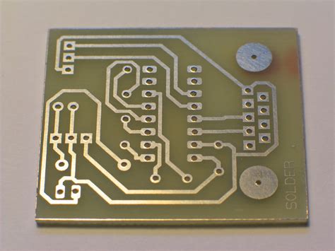
The following image shows an example of thermal reliefs and via stitching used in a high current PCB design:

Analysis and Verification
Thermal Analysis
Thermal analysis is an essential step in validating high current PCB designs. Some common thermal analysis techniques include:
– Basic hand calculations using thermal resistance models
– Computational fluid dynamics (CFD) simulations
– Finite element analysis (FEA)
– Thermal imaging of prototypes
The goal of thermal analysis is to ensure junction temperatures of components stay within safe limits and hot spots do not exceed the glass transition temperature of the PCB substrate.
Current Density Simulations
Current density simulations can be used to identify areas of high current concentration and potential voltage drop issues in PCB traces. These simulations calculate the current density and voltage at each point in the trace based on the geometry and applied current.
Some guidelines for acceptable current densities in PCB traces are:
– 10 A/mm² for normal operation
– 30 A/mm² for short-term transients
– 100 A/mm² for fusing current
Traces exceeding these thresholds may need to be widened or supplemented with additional copper layers.
EMC Testing and Certification
High current PCBs intended for commercial or industrial use may need to pass EMC testing and certification to ensure they do not cause electromagnetic interference with other equipment. Common EMC standards and certifications include:
– FCC Part 15B (USA)
– CISPR 22 (Europe)
– IEC 61000-4-x (immunity)
– MIL-STD-461 (military)
Pre-compliance testing during the design phase can help identify potential issues and avoid costly re-designs later.
Manufacturing Considerations
PCB Fabrication
High current PCBs may require specialized fabrication techniques and capabilities due to the thicker copper layers and larger feature sizes involved. Some key manufacturing considerations include:
– Minimum trace width and spacing
– Copper thickness and weight
– Hole size and plating thickness
– Solder mask and silkscreen clearances
– Panelization and routing
Close collaboration with the PCB fabricator is essential to ensure design requirements can be met and potential manufacturing issues are identified early.
Assembly and Soldering
The assembly and soldering process for high current PCBs must take into account the higher thermal mass of the thicker copper traces and the potential for elevated temperatures during reflow or wave soldering.
Some tips for successful assembly of high current boards include:
– Use thermally enhanced solder paste
– Increase solder stencil thickness
– Adjust reflow profile for higher peak temperatures
– Use selective soldering or point-to-point wiring for large components
– Provide adequate cooling during testing and burn-in
X-ray inspection and thermal imaging can be used to verify solder joint quality and identify any hot spots or thermal issues.
Frequently Asked Questions (FAQ)
What is considered a “high current” in PCB design?
There is no strict definition of “high current” in PCB design, but generally currents above 1-2 amps per trace would be considered high. However, even lower currents can cause thermal issues in small trace sizes or high-density designs.
How much voltage drop is acceptable in a high current PCB trace?
The maximum acceptable voltage drop depends on the application, but a general rule of thumb is to keep it below 0.5V or 5% of the supply voltage, whichever is lower. Excessive voltage drop can cause components to operate out of spec and generate additional heat.
What is the best way to reduce EMI in a high current PCB design?
Some effective techniques for reducing EMI in high current PCBs include:
– Minimizing high current loop areas
– Routing power and return paths close together
– Providing solid ground planes
– Using shielding and filtering on sensitive signals
– Placing high current traces away from board edges and openings
How do you calculate the current carrying capacity of a PCB trace?
The current carrying capacity of a PCB trace depends on factors such as the cross-sectional area, copper thickness, temperature rise, and ambient conditions. Various charts and calculators are available online to estimate trace current capacity. However, for high current designs, it’s best to perform detailed thermal simulations to ensure reliable operation.
What are some common mistakes to avoid in high current PCB layouts?
Some common mistakes to watch out for in high current PCB designs include:
– Undersizing traces or copper weights
– Routing high current traces near sensitive signals
– Neglecting thermal management and heat sinking
– Failing to provide adequate power decoupling and filtering
– Ignoring EMC considerations and skipping pre-compliance testing
By following best practices and performing thorough analysis and verification, these issues can be avoided and a robust high current PCB design can be achieved.
Conclusion
Designing PCBs for high current applications requires careful consideration of thermal management, voltage drop, EMI, and manufacturing constraints. By selecting appropriate components, using proper layout techniques, and performing detailed simulations and testing, reliable high current operation can be achieved. While the specific requirements and challenges will vary depending on the application, the general principles and practices outlined in this article can serve as a starting point for tackling high current PCB designs.
Leave a Reply