Introduction to PCB 3D Design
In the world of electronic design, Printed Circuit Boards (PCBs) play a crucial role in connecting and supporting electronic components. As technology advances and designs become more complex, the need for accurate and efficient PCB design has become increasingly important. This is where 3D functions come into play, revolutionizing the way PCB designers work.
What is PCB 3D Design?
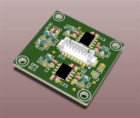
PCB 3D design is the process of creating a three-dimensional representation of a PCB, including all its components, layers, and traces. This virtual model allows designers to visualize the board from various angles, identify potential issues, and optimize the layout for manufacturing.
Benefits of Using 3D Functions in PCB Design
-
Improved Visualization: 3D functions provide a realistic representation of the PCB, making it easier for designers to understand the spatial relationships between components and traces.
-
Enhanced Collaboration: With 3D models, designers can easily share their work with team members, clients, and manufacturers, facilitating better communication and collaboration.
-
Early Error Detection: By visualizing the PCB in 3D, designers can identify potential issues, such as component collisions or insufficient clearances, early in the design process.
-
Optimized Manufacturing: 3D models help designers ensure that the PCB layout is optimized for manufacturing, reducing the risk of errors and delays during production.
Key Features of PCB 3D Design Software
To effectively utilize 3D functions in PCB design, designers rely on specialized software that offers a range of features and tools. Some of the key features of PCB 3D design software include:
1. 3D Modeling and Visualization
PCB 3D design software allows designers to create accurate 3D models of their boards, including all components, layers, and traces. These models can be rotated, zoomed, and manipulated to provide a comprehensive view of the design from any angle.
2. Component Libraries
Most PCB 3D design software comes with extensive libraries of 3D models for common electronic components. These libraries save designers time and effort by providing ready-to-use models that can be easily placed on the virtual board.
3. Collision Detection
3D design software often includes collision detection tools that automatically identify and highlight any instances where components or traces are intersecting or too close to each other. This feature helps designers avoid potential issues and ensures that the final design is error-free.
4. Design Rule Checking (DRC)
DRC is an essential feature in PCB 3D design software that checks the design against a set of predefined rules to ensure that it meets industry standards and manufacturing requirements. This includes checking for minimum clearances, trace widths, and other critical parameters.
5. Export Options
Once the 3D design is complete, PCB design software typically offers a range of export options, allowing designers to generate files suitable for manufacturing, such as Gerber files, drill files, and 3D models in various formats.

The Design Process with 3D Functions
Incorporating 3D functions into the PCB design process involves several key steps, each of which contributes to the creation of a successful, manufacturable board.
1. Schematic Design
The first step in the PCB design process is to create a schematic diagram that represents the electrical connections between components. This schematic serves as the foundation for the subsequent 3D design.
2. Component Placement
Once the schematic is complete, designers begin placing components on the virtual 3D board. This process involves selecting appropriate components from the software’s libraries and arranging them in a logical and efficient manner.
3. Trace Routing
With the components in place, designers then route the traces that connect them. 3D functions allow designers to visualize the traces in three dimensions, ensuring that they are properly spaced and avoid any obstacles or collisions.
4. Design Review and Optimization
After the initial layout is complete, designers use 3D functions to review the board from various angles, checking for any potential issues or areas for improvement. This may involve adjusting component placement, rerouting traces, or making other modifications to optimize the design.
5. Design Rule Checking and Export
Before finalizing the design, designers run DRC to ensure that the board meets all necessary standards and requirements. Once the design passes DRC, it can be exported in various formats for manufacturing.

Case Studies: Successful PCB 3D Designs
To better understand the impact of 3D functions on PCB design, let’s examine some real-world case studies where designers have successfully leveraged these tools to create innovative and efficient boards.
Case Study 1: Compact Medical Device
A medical device manufacturer needed to design a compact, high-density PCB for a new portable monitoring system. By using 3D functions, the design team was able to:
- Visualize the placement of components in a tight space
- Identify and resolve potential component collisions early in the design process
- Optimize the layout for manufacturability and reliability
The resulting PCB was 40% smaller than the company’s previous designs, while maintaining the same functionality and performance.
Case Study 2: High-Speed Telecommunications Equipment
A telecommunications equipment provider required a complex, multi-layer PCB for a new high-speed data processing unit. With the help of 3D functions, the design team:
- Created an accurate 3D model of the board, including all layers and components
- Simulated the high-speed signal paths to ensure optimal performance
- Collaborated effectively with the manufacturing team to streamline production
The final PCB design met all performance requirements and was successfully manufactured with minimal delays or issues.

The Future of PCB 3D Design
As technology continues to advance and electronic devices become increasingly complex, the role of 3D functions in PCB design will only grow in importance. Some of the trends and developments we can expect to see in the future include:
1. Integration with Augmented Reality (AR) and Virtual Reality (VR)
PCB 3D design software may soon incorporate AR and VR technologies, allowing designers to interact with their designs in immersive, three-dimensional environments. This could further enhance visualization and collaboration capabilities.
2. Increased Automation and AI-Assisted Design
As artificial intelligence (AI) and machine learning technologies advance, we can expect to see more automation in the PCB design process. AI-assisted tools may help designers optimize layouts, identify potential issues, and generate design variations based on specific criteria.
3. Seamless Integration with Manufacturing Processes
The future of PCB 3D design will likely involve even closer integration with manufacturing processes, allowing for a more seamless transition from design to production. This could include the use of 3D models for virtual prototyping, direct integration with manufacturing equipment, and real-time feedback loops between design and production teams.
FAQ
-
What is the main benefit of using 3D functions in PCB design?
The main benefit of using 3D functions in PCB design is the ability to visualize and optimize the board layout in a realistic, three-dimensional environment. This helps designers identify potential issues early, collaborate more effectively, and create designs that are optimized for manufacturing. -
Do I need special training to use PCB 3D design software?
While some training is helpful to fully leverage the capabilities of PCB 3D design software, most modern tools are designed to be intuitive and user-friendly. Many software providers offer tutorials, online resources, and support to help designers get started and develop their skills. -
How does PCB 3D design software integrate with other tools in the design process?
PCB 3D design software typically integrates with other tools, such as schematic capture software, through file import and export capabilities. Many software packages also offer direct integration with popular CAD tools, allowing for a more seamless design process. -
Can PCB 3D design software help with high-speed or RF design?
Yes, many PCB 3D design software packages include features specifically designed for high-speed and RF applications. These may include tools for simulating signal integrity, analyzing impedance, and optimizing trace routing for high-frequency signals. -
What should I look for when choosing PCB 3D design software?
When selecting PCB 3D design software, consider factors such as ease of use, compatibility with your existing tools and processes, the availability of component libraries, and the level of support and resources provided by the software vendor. It’s also important to choose software that meets the specific needs of your projects, such as support for high-speed design or advanced manufacturing capabilities.
Conclusion
The use of 3D functions in PCB design has revolutionized the way electronic products are developed, enabling designers to create more complex, efficient, and reliable boards. By leveraging the power of 3D visualization, collaboration, and optimization, PCB designers can streamline the design process, reduce errors, and bring innovative products to market faster than ever before.
As technology continues to evolve, the role of 3D functions in PCB design will only become more critical. By staying up-to-date with the latest tools, techniques, and best practices, designers can ensure that they are well-positioned to meet the challenges of the future and create the next generation of groundbreaking electronic devices.
Leave a Reply