Introduction to Through-hole Assembly
Through-hole assembly, also known as through-hole technology (THT), is a traditional method of assembling electronic components on a printed circuit board (PCB). This technique involves inserting the leads of components through drilled holes in the PCB and soldering them to pads on the opposite side. Despite the growing popularity of surface mount technology (SMT), through-hole assembly remains a crucial method for certain applications and components.
Advantages of Through-hole Assembly
- Mechanical strength: Through-hole components offer superior mechanical stability compared to surface-mounted components, as the leads are inserted through the board and soldered on the opposite side.
- Ease of manual assembly: Through-hole components are easier to handle and solder manually, making them ideal for prototyping, low-volume production, or hobbyist projects.
- High power handling: Through-hole components can handle higher power levels than their surface-mounted counterparts due to their larger size and better heat dissipation.
- Compatibility with legacy components: Some components, such as certain connectors, switches, and high-power devices, are only available in through-hole packages.
Disadvantages of Through-hole Assembly
- Lower component density: Through-hole components require more board space due to their larger size and the need for drilled holes, resulting in lower component density compared to SMT.
- Increased manufacturing time: Through-hole assembly is generally slower than SMT, as components need to be inserted manually or with specialized equipment, and the soldering process is more time-consuming.
- Higher cost for high-volume production: For large-scale production, through-hole assembly can be more expensive than SMT due to the increased labor and time required.
- Limited design flexibility: Through-hole components have fixed lead spacing and hole sizes, which can limit design flexibility compared to the more versatile SMT components.
Through-hole Assembly Process
The through-hole assembly process consists of several steps, each of which is crucial for ensuring the quality and reliability of the final product.
1. PCB Preparation
Before starting the assembly process, the PCB must be prepared with the necessary holes and pads for the through-hole components.
PCB Design
The PCB design stage involves creating a layout that accommodates the through-hole components, ensuring proper hole sizes, pad dimensions, and spacing between components. Designers must also consider factors such as power distribution, signal integrity, and thermal management.
PCB Fabrication
Once the design is finalized, the PCB is fabricated using a multi-step process that includes:
- Substrate preparation
- Copper cladding
- Photoresist application
- Exposure and development
- Etching
- Resist removal
- Drilling
- Plating
- Solder mask application
- Silkscreen printing
2. Component Placement
After the PCB is fabricated, the through-hole components are placed on the board either manually or using automated equipment.
Manual Placement
For low-volume production or prototyping, components are typically inserted by hand. This process requires skilled technicians who can accurately place the components in the correct orientation and position.
Automated Placement
In high-volume production, automated insertion machines are used to place through-hole components quickly and accurately. These machines use a variety of methods, such as axial, radial, or dip insertion, depending on the component type and packaging.
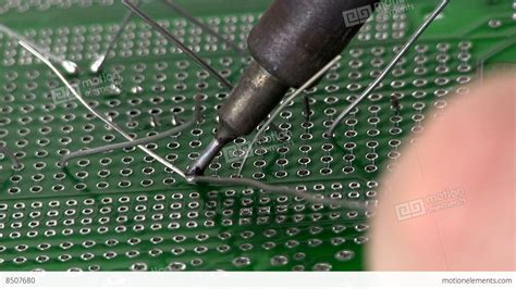
3. Soldering
Once the components are placed, the leads are soldered to the pads on the opposite side of the PCB to create an electrical and mechanical connection.
Manual Soldering
For manual soldering, a soldering iron is used to apply heat and solder to the component leads and pads. This method requires skill and experience to ensure proper solder joint formation and avoid defects such as bridging, cold joints, or insufficient solder.
Wave Soldering
Wave soldering is an automated process that is commonly used for through-hole assembly. In this method, the PCB with inserted components is passed over a molten solder wave, which selectively solders the component leads to the pads. Wave soldering is faster and more consistent than manual soldering but requires careful control of parameters such as solder temperature, conveyor speed, and flux application.
Selective soldering
Selective soldering is another automated method that uses a focused solder nozzle to apply solder to specific areas of the PCB. This technique is useful for boards with a mix of through-hole and surface-mounted components, or for components that are sensitive to the high temperatures of wave soldering.
4. Inspection and Testing
After soldering, the assembled PCBs undergo inspection and testing to ensure the quality and functionality of the final product.
Visual Inspection
Visual inspection is the first step in the quality control process. Technicians examine the solder joints, component placement, and overall board condition for defects such as bridging, tombstoning, or missing components.
Automated Optical Inspection (AOI)
AOI systems use cameras and image processing algorithms to automatically detect and classify assembly defects. This method is faster and more consistent than manual visual inspection and can identify defects that may be difficult to spot with the naked eye.
X-ray Inspection
X-ray inspection is used to examine solder joints and components that are hidden from view, such as those underneath ball grid array (BGA) packages or within connectors. This non-destructive method can detect voids, cracks, or other internal defects that may affect the reliability of the assembly.
Electrical Testing
Electrical testing is performed to verify the functionality and performance of the assembled PCB. This may include:
- In-circuit testing (ICT): Probes are used to test individual components and circuits on the board.
- Functional testing: The PCB is powered on and tested under various operating conditions to ensure proper functionality.
- Boundary scan testing: A built-in self-test method that uses a special test access port (TAP) to test interconnects and components on the board.

Component Types and Packages
Through-hole components come in various types and packages, each with its own characteristics and applications.
Axial Components
Axial components have leads that extend from opposite ends of the component body, along its axis. Examples include:
- Resistors
- Capacitors
- Inductors
- Diodes
Radial Components
Radial components have leads that extend from the same side of the component body, perpendicular to its axis. Examples include:
- Electrolytic capacitors
- Ceramic capacitors
- LEDs
DIP (Dual In-line Package) Components
DIP components have two parallel rows of leads extending from the bottom of the component body. Examples include:
- Integrated circuits (ICs)
- Sockets
- Headers

Design Considerations for Through-hole Assembly
When designing a PCB for through-hole assembly, several factors must be considered to ensure manufacturability, reliability, and functionality.
Hole Size and Pad Dimensions
The hole size and pad dimensions must be appropriate for the component leads to ensure a proper fit and adequate soldering. The hole size should be slightly larger than the lead diameter to allow for insertion tolerances, while the pad size should be large enough to accommodate the solder fillet and provide sufficient mechanical strength.
Lead Spacing and Pitch
Lead spacing, or pitch, refers to the distance between the centers of adjacent leads on a component. Designers must ensure that the lead spacing is compatible with the PCB layout and allows for proper soldering and inspection.
Component Orientation and Placement
Component orientation and placement should be clearly indicated on the PCB layout and assembly drawings to avoid mistakes during manual or automated insertion. Proper component spacing and orientation also help to ensure adequate clearance for soldering and inspection.
Thermal Management
Through-hole components, especially those handling high power levels, may generate significant heat during operation. Designers must consider thermal management strategies, such as using larger pads, thermal vias, or heat sinks, to dissipate heat and prevent component failure or PCB damage.
Manufacturability and Cost
When designing for through-hole assembly, it is essential to consider the manufacturability and cost implications of the design choices. Factors such as component selection, board size, layer count, and drilling requirements can impact the assembly time, equipment needs, and overall cost of the project.

Best Practices for Through-hole Assembly
To ensure the success of a through-hole assembly project, follow these best practices:
- Use consistent and clear component designators and polarity markers on the PCB layout and assembly drawings.
- Specify the correct component types, values, and packages in the bill of materials (BOM) and assembly documentation.
- Follow industry standards and guidelines for hole sizes, pad dimensions, and lead spacing to ensure compatibility and manufacturability.
- Use appropriate soldering techniques and materials, such as the correct solder alloy, flux, and temperature settings, to achieve reliable solder joints.
- Implement proper inspection and testing procedures to identify and correct assembly defects early in the process.
- Provide adequate training and resources for assembly personnel to ensure consistent quality and efficiency.
- Regularly review and update assembly processes and documentation to incorporate new technologies, best practices, and lessons learned.
Troubleshooting Common Through-hole Assembly Issues
Despite best efforts, issues may arise during the through-hole assembly process. Some common problems and their potential solutions include:
Solder Bridges
Solder bridges occur when excess solder inadvertently connects adjacent pads or leads.
- Solutions: Use appropriate soldering techniques, such as controlling solder volume and temperature; use solder masks to prevent bridging; remove bridges with solder wick or a desoldering tool.
Cold Solder Joints
Cold solder joints are dull, grainy, or incomplete connections that result from insufficient heat or poor wetting.
- Solutions: Ensure proper soldering temperature and dwell time; use fresh, clean solder and flux; preheat the PCB and components if necessary; rework cold joints with additional solder and heat.
Tombstoning
Tombstoning occurs when a component stands up on one end due to uneven heating or surface tension during soldering.
- Solutions: Ensure even heating of component leads; use appropriate pad sizes and solder volumes; adjust component placement and orientation to minimize tombstoning risk.
Insufficient Solder Fillets
Insufficient solder fillets are weak or incomplete connections that result from too little solder or poor wetting.
- Solutions: Use adequate solder volume; ensure proper soldering temperature and dwell time; clean and prep component leads and pads for better wetting; rework with additional solder as needed.
Conclusion
Through-hole assembly remains an essential method for producing reliable, high-quality electronic assemblies, particularly for applications that require strong mechanical connections, high power handling, or compatibility with legacy components. By understanding the process, design considerations, best practices, and common issues associated with through-hole assembly, designers and manufacturers can successfully implement this traditional PCB assembly technique in their projects.
As technology advances and new components and packaging options emerge, it is crucial to stay informed about the latest developments and adapt through-hole assembly processes accordingly. By combining the proven reliability of through-hole technology with modern design and manufacturing techniques, electronic products can continue to meet the evolving demands of industries and consumers alike.
Frequently Asked Questions (FAQ)
1. What is the difference between through-hole and surface-mount assembly?
Through-hole assembly involves inserting component leads through drilled holes in the PCB and soldering them to pads on the opposite side, while surface-mount assembly places components directly onto pads on the PCB surface and solders them in place. Through-hole components are generally larger and offer stronger mechanical connections, while surface-mount components enable higher component density and faster assembly.
2. Can through-hole and surface-mount components be used on the same PCB?
Yes, PCBs can be designed to accommodate both through-hole and surface-mount components, known as a mixed-technology or hybrid assembly. However, this approach may require special design considerations and assembly processes to ensure compatibility and reliability.
3. What are the most common through-hole component packages?
The most common through-hole component packages include axial (resistors, capacitors, diodes), radial (capacitors, LEDs), and DIP (integrated circuits, sockets, headers).
4. How do I select the appropriate hole size and pad dimensions for through-hole components?
Hole size and pad dimensions should be selected based on the component lead diameter and soldering requirements. Typically, the hole size should be 0.2-0.5 mm larger than the lead diameter, and the pad should be at least 1.5-2 times the hole size to ensure adequate solder fillets and mechanical strength. Consult component datasheets and industry standards for specific recommendations.
5. What are some common challenges associated with through-hole assembly, and how can they be addressed?
Common challenges in through-hole assembly include solder bridges, cold solder joints, tombstoning, and insufficient solder fillets. These issues can be addressed by using appropriate soldering techniques, controlling solder volume and temperature, ensuring proper component placement and orientation, and implementing thorough inspection and rework processes. Regular training and process improvements can also help minimize these challenges.
Leave a Reply