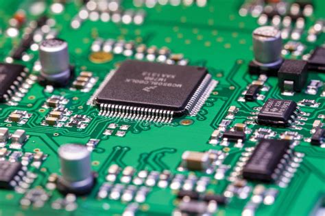
What are Printed Circuit Boards?
PCBs are flat boards made of insulating materials, such as fiberglass or plastic, with conductive pathways etched onto them. These pathways, also known as traces, connect various electronic components, such as resistors, capacitors, and integrated circuits (ICs), to form a complete electronic circuit. PCBs provide a stable and reliable platform for these components to be mounted and connected, allowing for the efficient transfer of electrical signals and power.
Types of PCBs
There are several types of PCBs, each designed for specific applications and requirements. The most common types include:
- Single-sided PCBs: These have conductive traces on only one side of the board and are typically used in simple, low-cost electronic devices.
- Double-sided PCBs: These have conductive traces on both sides of the board, allowing for more complex circuits and higher component density.
- Multi-layer PCBs: These consist of multiple layers of conductive traces separated by insulating layers, enabling even more complex circuits and higher component density.
- Flexible PCBs: These are made of flexible materials, such as polyimide, and can be bent or folded to fit into tight spaces or conform to specific shapes.
- Rigid-Flex PCBs: These combine the benefits of both rigid and flexible PCBs, allowing for the integration of multiple circuit boards into a single, compact assembly.
| Type of PCB | Layers | Complexity | Cost | Applications |
|---|---|---|---|---|
| Single-sided | 1 | Low | Low | Simple, low-cost devices |
| Double-sided | 2 | Medium | Medium | More complex devices, higher component density |
| Multi-layer | 3+ | High | High | Complex devices, high component density |
| Flexible | 1-2 | Medium | Medium | Wearables, compact devices, curved surfaces |
| Rigid-Flex | 2+ | High | High | Complex, compact devices, multi-board assemblies |
The Manufacturing Process of PCBs
The manufacturing process of PCBs involves several steps, each requiring precision and attention to detail. The main steps in the PCB manufacturing process are:
- Design: The PCB design is created using specialized software, such as Altium Designer or Eagle, which generates the necessary files for manufacturing.
- Printing: The PCB design is printed onto a copper-clad board using a photoresist layer and exposed to UV light, creating a pattern of the circuit traces.
- Etching: The exposed copper is removed using a chemical etching process, leaving only the desired conductive traces on the board.
- Drilling: Holes are drilled into the board to accommodate through-hole components and allow for the connection of layers in multi-layer PCBs.
- Plating: The holes are plated with a conductive material, such as copper, to ensure proper electrical connections between layers.
- Solder Mask Application: A protective layer, known as a solder mask, is applied to the board to prevent accidental short circuits and provide insulation between components.
- Silkscreen Printing: Text, symbols, and logos are printed onto the board using a silkscreen process for easy identification of components and assembly instructions.
- Surface Finishing: A surface finish, such as HASL (Hot Air Solder Leveling) or ENIG (Electroless Nickel Immersion Gold), is applied to the exposed copper to prevent oxidation and improve solderability.
- Assembly: Electronic components are mounted onto the PCB using various techniques, such as through-hole or surface-mount technology (SMT), and soldered in place.
- Testing and Inspection: The assembled PCB undergoes rigorous testing and inspection to ensure proper functionality and adherence to quality standards.

Applications of PCBs in Various Industries
PCBs are used in a wide range of industries due to their versatility, reliability, and ability to support complex electronic circuits. Some of the key industries that rely heavily on PCBs include:
Consumer Electronics
PCBs are the foundation of consumer electronic devices, such as smartphones, tablets, laptops, and televisions. The high component density and compact design of PCBs enable manufacturers to create increasingly smaller and more powerful devices with each generation.
Automotive Industry
Modern vehicles incorporate numerous electronic systems, such as engine control units (ECUs), infotainment systems, and advanced driver assistance systems (ADAS). PCBs play a crucial role in the functioning and integration of these systems, enabling safer, more efficient, and more connected vehicles.
Medical Devices
PCBs are essential components in a wide range of medical devices, from patient monitoring systems and diagnostic equipment to implantable devices and surgical instruments. The reliability and precision of PCBs are critical in ensuring the safety and effectiveness of these life-saving devices.
Aerospace and Defense
PCBs used in aerospace and defense applications must meet stringent requirements for reliability, durability, and performance under extreme conditions. High-quality PCBs are essential for the proper functioning of avionics systems, communication equipment, and weapons systems.
Industrial Automation
PCBs are at the heart of industrial automation systems, enabling the control and monitoring of manufacturing processes, robotics, and machine-to-machine communication. The ruggedness and reliability of industrial-grade PCBs ensure the smooth operation of these critical systems.

The Future of PCBs
As technology continues to advance, the demand for more sophisticated and compact electronic devices will only increase. This will drive the development of new PCB Technologies and manufacturing processes, such as:
- Embedded components: Integrating passive components, such as resistors and capacitors, directly into the PCB substrate, reducing the size and complexity of the overall assembly.
- High-Density Interconnect (HDI) PCBs: Utilizing smaller via sizes and finer trace widths to achieve even higher component density and more compact designs.
- 3D printing: Leveraging additive manufacturing techniques to create complex, three-dimensional PCB structures with embedded components and interconnects.
- Advanced materials: Incorporating new materials, such as graphene or ceramic substrates, to improve the thermal, electrical, and mechanical properties of PCBs.
As these technologies mature, we can expect to see even more innovative and powerful electronic devices that rely on the continued development and importance of PCBs.

Frequently Asked Questions (FAQ)
- What is the difference between a PCB and a printed wiring board (PWB)?
- A PCB and a PWB are essentially the same things. The term “printed wiring board” is an older term that was used before the advent of modern PCB manufacturing techniques. Today, the term “printed circuit board” is more widely used and encompasses both the wiring and the components mounted on the board.
- What are the advantages of using a multi-layer PCB?
- Multi-layer PCBs offer several advantages, including higher component density, improved signal integrity, reduced electromagnetic interference (EMI), and better thermal management. By utilizing multiple layers, designers can create more complex circuits in a smaller footprint while minimizing signal crosstalk and interference.
- What is the purpose of the solder mask on a PCB?
- The solder mask is a protective layer applied to the surface of a PCB to prevent accidental short circuits and provide insulation between components. It also helps to prevent solder bridging during the assembly process and protects the copper traces from oxidation and other environmental factors.
- How do I choose the right type of PCB for my application?
- Choosing the right type of PCB depends on several factors, such as the complexity of the circuit, the required component density, the operating environment, and the budget. Single-sided and double-sided PCBs are suitable for simpler, low-cost applications, while multi-layer and flexible PCBs are better suited for more complex, high-density designs. Consulting with a PCB manufacturer or design expert can help you make the best choice for your specific application.
- What are the environmental concerns associated with PCB manufacturing and disposal?
- PCB manufacturing involves the use of various chemicals and materials that can be harmful to the environment if not properly managed. These include heavy metals, such as lead and copper, as well as organic solvents used in the etching and cleaning processes. Proper disposal of PCBs is also critical, as they can release toxic substances if not recycled or disposed of correctly. Responsible PCB manufacturers adhere to strict environmental regulations and implement best practices to minimize their ecological impact, such as using lead-free materials and properly treating wastewater.
In conclusion, PCBs are indispensable components in the world of electronics, enabling the creation of increasingly sophisticated and powerful devices across a wide range of industries. As technology continues to evolve, so too will the design and manufacturing of PCBs, driving innovation and shaping the future of electronic devices. By understanding the importance of PCBs and their role in modern electronics, we can better appreciate the technological marvels that surround us and the potential for future advancements in this exciting field.
Leave a Reply