Introduction
Radio frequency (RF) printed circuit board (PCB) design requires careful planning and execution to achieve optimal performance. This article provides an overview of key considerations for RF PCB design.
RF System Design
The first step in any RF PCB design project is to fully understand the RF system requirements. This includes parameters like:
- Operating frequencies
- Bandwidth
- Output power
- Noise figure
- Linearity
These specifications will guide the PCB stackup, layout, and component selection.
Stackup Design

The PCB stackup, which refers to the sequence and properties of the dielectric and metal layers, is critical for RF performance. Key stackup considerations include:
Layer Count
More layers provide better isolation and allow for short, direct routing. 4-8 layers are typical for RF boards.
Dielectric Materials
Low-loss substrates (Rogers, Taconic) are preferred. Dielectric constant impacts impedance control.
Layer Thickness
Thicker dielectric layers reduce crosstalk and radiation loss. But thin layers help with impedance control.
Buried Vias
Help isolate analog and digital sections. Require additional board layers.
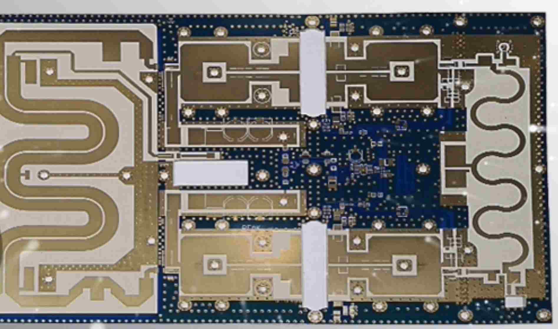
Layout Guidelines
Proper layout is essential for achieving good RF performance. Here are some key guidelines:
- Keep trace lengths as short as possible
- Use large package components to allow short connections
- Minimize the number of vias, which add inductance
- Use surface mounted devices instead of through-hole
- Provide proper grounding and equal-potential planes
- Isolate analog and digital sections
- Maintain constant impedance for matched transmission lines
- Avoid 90° angles for transmission lines
Component Selection
Choose appropriate RF components like connectors, capacitors, resistors, transistors and integrated circuits (ICs). Key factors are operating frequency range, parasitic effects, and packaging.
Simulation and Tuning
Use 3D EM simulation tools to model the PCB layout. Tune the design by tweaking layout, stackup, component values and placement. Measure prototypes and correlate with simulations.
Frequently Asked Questions
What are some key substrate materials used in RF PCBs?
Some common substrate materials are Rogers RO4003C and RO4350B, Taconic RF-35 and RF-60A, and FR-4. Rogers and Taconic substrates provide tight dielectric constant tolerances and low loss for high frequency applications. FR-4 can be used for less demanding designs.
What is a rule of thumb for RF trace width?
As a general rule, RF trace width should be at least 3x the dielectric thickness. For a common 4 mil dielectric, traces would be 12 mils wide at a minimum. Wider traces reduce loss.
How can crosstalk be minimized in an RF PCB?
Using thicker dielectrics, buried vias, shielding, differential pairs, and avoiding parallel traces for different signals can all help reduce crosstalk. Proper stackup design is key.
What are some PCB finishes suitable for RF boards?
Common finishes include immersion silver, immersion tin, ENIG (electroless nickel immersion gold), and OSP (organic solderability preservative). Silver provides the best conductivity. ENIG offers a good balance of cost and performance.
How can vias be de-tuned in an RF design?
Back-drilling, using blind/buried vias, and filling vias with epoxy are common techniques. This reduces the via stub length which helps mitigate their parasitic effects.
Leave a Reply