Key Considerations for RF Microwave PCB Design
As technology continues to advance, there is an increasing demand for smaller, faster, and more efficient electronics. This is especially true for wireless devices that rely on radio frequency (RF) and microwave signals to transmit data. Proper printed circuit board (PCB) design is critical for the successful operation of these high-frequency circuits. Here are some key considerations when designing PCBs for RF and microwave applications:
Impedance Control
Maintaining proper impedance matching and control is crucial in RF/microwave design. Signals traveling through transmission lines will reflect and cause interference if the impedance changes. Use controlled impedance PCB materials and carefully match components and trace widths to the desired impedance. This will minimize loss, reflections, and echoes.
Signal Integrity
At high frequencies, issues like crosstalk, ground bounce, and electromagnetic interference (EMI) are major concerns. Proper stackup design, grounding techniques, decoupling, and isolation between critical traces safeguards signal integrity. Simulating the PCB layout is also important to identify potential problems.
Transmission Lines
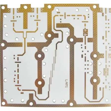
Controlled impedance transmission lines like microstrip, stripline, and coplanar waveguide are commonly used on RF/microwave PCBs. The dimensions and materials of these transmission lines must be carefully selected to achieve the characteristic impedance needed. Discontinuities alter impedance and should be minimized.
Passive Components
Passive components like resistors, capacitors, and inductors behave differently at high frequencies. Pay attention to parameters like Equivalent Series Resistance (ESR), Self Resonant Frequency (SRF), and Q factor when selecting RF/microwave passive parts. High frequency passives require special design consideration.
Materials and Finishes

Use PCB materials like FR4 or polyimide with stable electrical properties at microwave frequencies. Low-loss dielectric materials are preferred. Smooth copper finishes allow better performance for high-speed signals. Some RF/microwave boards may require exotic materials like Teflon or Rogers.<br> <h2>RF Microwave PCB Layout and Routing</h2>
Proper PCB layout and routing is key for RF and microwave design success. Here are some layout techniques and principles to follow:
- Place components strategically to minimize trace lengths
- Group components by function into separate sections
- Use 45° angles instead of 90° angles for traces and component placement where possible
- Avoid sharp bends, stubs, and T-junctions on transmission lines
- Route critical traces over a ground plane for controlled impedance and EMI shielding
- Use voids in the ground plane under traces that need isolation
- Carefully position and isolate RF input/output ports
- Use coplanar waveguides for ultra-high frequency routing
- Simulate layouts with 3D EM field solvers to verify performance
- Follow any specific layout rules given for critical active components
- Allow enough spacing between traces and components for the frequency
- Use stitching vias along transmission lines for RF return paths
Paying close attention to these PCB layout considerations for RF and microwave frequencies allows for success across wireless applications including 5G, radars, satellites, medical systems and more. Simulation, modeling, and prototyping is key to verifying layouts meet all electrical requirements.<h2>Manufacturing and Testing RF Microwave PCBs</h2>
Once the PCB layout is complete, careful attention during manufacturing and testing helps achieve optimal RF/microwave performance. Here are some important manufacturing guidelines:
- Work with a PCB manufacturer experienced in RF/microwave boards
- Use tight process controls and tolerances for trace widths and distances
- Validate electrical performance of materials used such as dielectric constant
- Ensure excellent copper surface finish for high frequency conductors
- Carry out thorough impedance testing for controlled impedance circuits
- Perform extensive RF/microwave testing like insertion loss, return loss, and isolation
- Verify frequency performance across full range – DC to 50+ GHz
- Debug and improve designs that fail to meet RF performance targets
- Execute shock, vibration, and thermal cycling to ensure robustness
Prototyping, testing, and iterating is key to realizing a successful RF microwave PCB. Careful design, layout, manufacturing, and testing results in boards that function well across a wide frequency range.<h2>Applications and Examples of RF Microwave PCBs</h2>
RF and microwave PCB technology enables many important applications and products including:
- 5G NR base stations and infrastructure – 5G employs frequencies up to 40 GHz for huge bandwidth. Careful PCB design and layout is needed.
- Satellites – Satellite communication uses microwave bands from 3 GHz to 300 GHz for data links. Circuits must maintain signal integrity in space.
- Radar systems – Many radar systems operate at microwave frequencies from 1 to 40 GHz. Stable PCB materials and layout prevents signal degradation.
- Wireless medical devices – Medical products like MRI machines use RF PCBs working up to 500 MHz for imaging and diagnosis.
- Automotive radar – Vehicles employ 77 GHz and 24 GHz radar with RF PCBs designed for collision detection and avoidance.
- High-speed data links – Backplanes, data centers, test equipment and more need RF PCBs to work at multi-Gb/s speeds with low loss.
- IoT devices – Wearables, sensors, and other IoT products use ISM bands like 2.4 GHz and 5 GHz requiring optimized RF PCB design.
- Aerospace/Defense – Avionics, electronic warfare systems, communications platforms utilize microwave PCB technology extensively.
With the right design and manufacturing approach, RF and microwave PCBs will continue serving these critical applications for years to come.<h2>Frequently Asked Questions</h2>
Q: What are some key differences between RF PCBs and regular PCBs?
A: RF PCBs require much more attention to impedance control, transmission lines, specialty materials, EMI control, and layout techniques compared to regular PCBs due to the high frequencies involved.
Q: What are some special analysis done for RF PCBs?
A: Important RF analyses like signal integrity simulations, electromagnetic field solvers, and thermal analysis help verify performance. Shock/vibration/temperature analysis ensures reliability.
Q: What fab and assembly challenges are there with RF PCBs?
A: Tolerances are much tighter – 2-3 mils lines/spaces are common. Materials must perform well at high frequencies. Many precise RF tests are required. Passives must be properly matched and tuned.
Q: What are some ways to reduce losses in an RF PCB?
A: Use low-loss PCB materials, avoid 90 degree bends, minimize trace lengths, use wider traces, utilize ground planes, and select proper passive components rated for RF.
Q: How can I isolate sensitive RF circuits from noise sources?
A: Strategic use of ground planes, guards, spacing, bandpass filters, shielding enclosures/cans, and low-noise circuit design helps protect RF circuits from interference.
Leave a Reply