What is a PCB Trace?
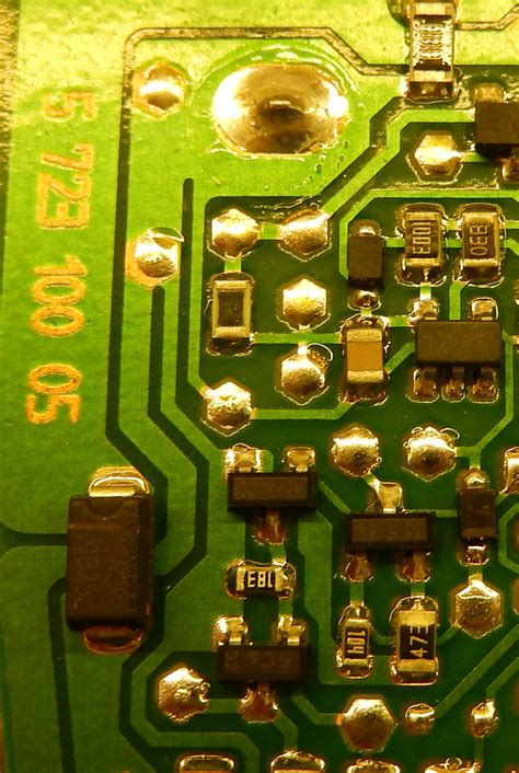
A PCB trace, also known as a copper trace or a track, is a conductive pathway on a printed Circuit Board (PCB) that electrically connects different components. These traces are essential for the functioning of any electronic device, as they allow signals and power to be routed between components such as resistors, capacitors, integrated circuits, and connectors.
PCB traces are typically made of copper, which is an excellent conductor of electricity. The copper layer is laminated onto a non-conductive substrate, such as FR-4, which provides mechanical support and insulation between the traces.
The Importance of PCB Traces
PCB traces play a crucial role in the performance and reliability of electronic devices. Some of the key reasons why PCB traces are important include:
-
Signal Integrity: Well-designed PCB traces ensure that signals are transmitted accurately and efficiently between components, minimizing signal distortion, crosstalk, and electromagnetic interference (EMI).
-
Power Distribution: PCB traces are responsible for distributing power from the power source to various components on the board. Properly designed power traces ensure that each component receives the correct voltage and current, while minimizing voltage drops and power losses.
-
Electromagnetic Compatibility (EMC): Carefully routed PCB traces help to minimize electromagnetic interference (EMI) and ensure that the device complies with EMC regulations.
-
Manufacturability: Well-designed PCB traces make the manufacturing process more efficient and reliable, reducing the likelihood of defects and improving yield.

Design Considerations for PCB Traces
When designing PCB traces, several factors must be considered to ensure optimal performance and reliability. Some of these factors include:
Trace Width
The width of a PCB trace determines its current-carrying capacity and resistance. Wider traces can carry more current and have lower resistance, but they also take up more space on the board. The appropriate trace width depends on factors such as the current requirements of the connected components, the available board space, and the manufacturing capabilities.
Here’s a table showing some common trace widths and their corresponding current-carrying capacities for 1 oz. copper (35 µm thickness) at various temperature rises:
| Trace Width (mm) | Current Capacity (A) at 10°C Rise | Current Capacity (A) at 20°C Rise | Current Capacity (A) at 30°C Rise |
|---|---|---|---|
| 0.25 | 0.5 | 0.7 | 0.9 |
| 0.5 | 1.0 | 1.4 | 1.7 |
| 1.0 | 2.0 | 2.8 | 3.4 |
| 2.0 | 4.0 | 5.7 | 6.8 |
| 3.0 | 6.0 | 8.5 | 10.2 |
Trace Spacing
The spacing between PCB traces is important for preventing short circuits and minimizing crosstalk between signals. The minimum trace spacing depends on factors such as the manufacturing capabilities, the voltage difference between adjacent traces, and the required insulation properties.
Here’s a table showing some common trace spacing guidelines for various voltage levels:
| Voltage (V) | Minimum Trace Spacing (mm) |
|---|---|
| <50 | 0.2 |
| 50-100 | 0.3 |
| 100-150 | 0.5 |
| 150-300 | 1.0 |
| >300 | 2.0 |
Trace Routing
The way PCB traces are routed can significantly impact signal integrity, EMI, and manufacturability. Some key considerations for trace routing include:
- Keeping signal traces as short and direct as possible to minimize signal delay and distortion
- Avoiding sharp corners and using smooth curves to minimize reflections and impedance discontinuities
- Separating sensitive signals from noisy traces to prevent crosstalk
- Using ground planes and power planes to provide shielding and reduce EMI
- Following manufacturing guidelines for minimum trace widths, spacings, and drill hole sizes
Impedance Control
For high-speed signals, it’s important to control the impedance of PCB traces to ensure proper signal integrity. Impedance is determined by factors such as the trace width, thickness, and spacing, as well as the dielectric properties of the PCB Substrate.
Common Controlled Impedance values include:
- 50 Ω for single-ended signals (e.g., coAXIal cables)
- 100 Ω for differential signals (e.g., USB, Ethernet)
To achieve controlled impedance, PCB designers use specialized software to calculate the required trace dimensions and spacing based on the substrate properties and desired impedance value.

PCB Trace Materials
While copper is the most common material for PCB traces, there are other materials that can be used in specific applications:
-
Gold: Gold-plated traces are sometimes used in high-reliability applications or for contacts that require frequent mating cycles, as gold is more resistant to corrosion and wear than copper.
-
Aluminum: Aluminum traces are occasionally used in high-power applications or for heat dissipation, as aluminum has a lower electrical conductivity but a higher thermal conductivity than copper.
-
Carbon Nanotubes: Research is ongoing into the use of carbon nanotubes as a potential replacement for copper traces in future PCBs, as they offer high electrical and thermal conductivity, as well as excellent mechanical strength.

PCB Trace Manufacturing Processes
PCB traces are typically created using a combination of etching and plating processes. The most common methods include:
-
Subtractive Process: In this method, a copper-clad substrate is coated with a photoresist, which is then exposed to UV light through a patterned mask. The unexposed photoresist is removed, and the exposed copper is etched away using chemicals, leaving only the desired traces.
-
Additive Process: This method involves selectively depositing copper onto a non-conductive substrate using techniques such as electroless plating or direct printing. This process can create finer traces and spaces compared to the subtractive process but is generally more expensive.
-
Semi-Additive Process (SAP): SAP is a hybrid of the subtractive and additive processes, where a thin layer of copper is deposited onto the substrate, patterned using photoresist, and then selectively plated to the desired thickness. This method combines the advantages of both processes, enabling fine features and high-density designs.
PCB Trace Inspection and Testing
To ensure the quality and reliability of PCB traces, various inspection and testing methods are employed during and after the manufacturing process. Some common techniques include:
-
Visual Inspection: PCBs are visually inspected for defects such as shorts, opens, and incorrect trace widths or spacings using microscopes or Automated Optical Inspection (AOI) systems.
-
Electrical Testing: Continuity and isolation tests are performed to verify that traces are correctly connected and not shorting to adjacent traces or planes. Flying probe testers or bed-of-nails fixtures are commonly used for this purpose.
-
X-Ray Inspection: X-ray imaging is used to inspect traces and vias in multi-layer PCBs, as these features are not visible from the surface.
-
Time-Domain Reflectometry (TDR): TDR is used to measure the impedance and locate faults in PCB traces by sending a high-frequency signal along the trace and analyzing the reflected waveform.
-
Thermal Imaging: Thermal cameras can be used to identify hot spots on the PCB caused by high-current traces or poor thermal management, helping to prevent reliability issues.
Frequently Asked Questions (FAQ)
1. What is the difference between a PCB trace and a via?
A PCB trace is a conductive pathway that runs along the surface of a PCB layer, while a via is a conductive hole that connects traces on different layers of the PCB.
2. Can PCB traces be repaired if damaged?
Yes, PCB traces can be repaired using techniques such as soldering, conductive epoxy, or wire jumpers, depending on the extent and location of the damage. However, it’s always best to prevent damage through careful handling and proper design.
3. How do I calculate the maximum current a PCB trace can handle?
The maximum current a PCB trace can handle depends on factors such as the trace width, thickness, and the allowable temperature rise. You can use online calculators or refer to IPC-2152 standards to determine the current-carrying capacity of a trace based on these parameters.
4. What is the difference between a single-ended and differential PCB trace?
A single-ended PCB trace carries a signal referenced to a common ground, while a differential PCB trace consists of a pair of traces carrying equal and opposite signals. Differential traces are used for high-speed, noise-sensitive applications, as they offer better noise immunity and signal integrity compared to single-ended traces.
5. Can PCB traces be used for antenna design?
Yes, PCB traces can be used to create antennas for wireless applications, such as Wi-Fi, Bluetooth, or NFC. These antennas are typically designed as specific shapes and sizes on the PCB to achieve the desired frequency and radiation characteristics. However, designing PCB trace antennas requires careful consideration of factors such as trace impedance, substrate properties, and surrounding components to ensure optimal performance.
Conclusion
PCB traces are the backbone of any electronic device, providing the vital connections between components that enable the device to function. Proper design, manufacturing, and testing of PCB traces are essential for ensuring the performance, reliability, and manufacturability of the final product.
As electronic devices continue to become smaller, faster, and more complex, the demands on PCB trace design and manufacturing will only increase. Staying up-to-date with the latest technologies, standards, and best practices is crucial for engineers and manufacturers to meet these challenges and create innovative, high-quality products.
Leave a Reply