Understanding PCB Panels
A PCB panel, also known as a PCB array, is a larger board that consists of multiple identical or different PCB designs arranged in a specific layout. The individual PCBs, called “circuit boards” or “cards,” are connected to the panel through small tabs or “break-off” points. After the assembly process is complete, the individual boards are separated from the panel by breaking or cutting along these designated points.
PCB paneling offers several advantages, including:
- Increased production efficiency
- Reduced handling and assembly time
- Lower manufacturing costs
- Improved consistency and quality control
Key Considerations for PCB Paneling
When designing and preparing PCB panels for assembly, there are several key factors to consider to ensure optimal results. Let’s explore these considerations in detail.
Panel Size and Shape
The size and shape of the PCB panel play a crucial role in the paneling process. The panel dimensions must be compatible with the manufacturing equipment and assembly processes used. Standard panel sizes vary depending on the fabrication facility and the specific requirements of the project.
Common panel sizes include:
| Panel Size | Dimensions (mm) |
|---|---|
| Small | 100 x 100 |
| Medium | 200 x 200 |
| Large | 300 x 300 |
| Extra Large | 450 x 450 |
It’s important to consult with your PCB manufacturer to determine the optimal panel size for your specific project. They can provide guidance based on their equipment capabilities and the complexity of your PCB design.
Panel Material and Thickness
The choice of panel material and thickness is another critical consideration. The most common materials used for PCB panels are:
- FR-4: A flame-retardant glass-reinforced epoxy laminate
- Aluminum: Used for metal-core PCBs (MCPCBs) for better thermal dissipation
- Polyimide: Used for flexible PCBs (FPCBs)
The thickness of the panel material depends on the number of layers in the PCB design and the desired rigidity of the final product. Standard PCB thicknesses range from 0.4mm to 3.2mm, with 1.6mm being the most common. Thicker panels provide better stability and durability but may increase manufacturing costs.
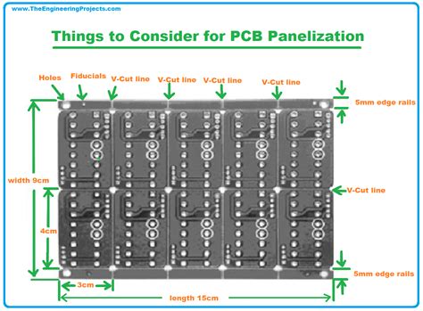
Panelization Layout and Spacing
The layout and spacing of the individual PCBs within the panel are crucial for proper assembly and separation. Here are some key considerations:
-
Board Orientation: The orientation of the boards should be consistent and aligned to facilitate automated assembly processes. Boards can be arranged in a horizontal, vertical, or mixed orientation depending on their shape and size.
-
Spacing Between Boards: Adequate spacing between the individual boards is necessary to prevent interference during assembly and to allow for clean separation after the process. The recommended minimum spacing is typically 2-3mm, but it can vary based on the manufacturing capabilities and the specific design requirements.
-
Fiducial Markers: Fiducial markers are reference points placed on the panel to assist in aligning and positioning the boards during automated assembly. These markers should be clearly visible and properly positioned to ensure accurate placement of components.
-
Tooling Holes: Tooling holes are used to secure the panel during the fabrication and assembly processes. The size, shape, and location of these holes should be consistent across the panel and compatible with the manufacturing equipment.
Tab and Break-off Point Design
The tabs and break-off points that connect the individual PCBs to the panel require careful design consideration. The main objectives are to ensure secure attachment during assembly while allowing for clean and easy separation afterward.
Here are some guidelines for tab and break-off point design:
-
Tab Width: The width of the tabs should be sufficient to hold the boards securely in place during assembly. A minimum tab width of 1-2mm is typically recommended, but it may vary based on the size and weight of the individual boards.
-
Tab Placement: Tabs should be placed strategically to provide balanced support and prevent warping or distortion of the boards. Placing tabs at the corners and along the edges of the boards is a common approach.
-
Break-off Point Design: The break-off points, also known as “mouse bites” or “v-grooves,” are perforations or weakened areas that allow for easy separation of the boards from the panel. The design of these points should ensure clean breakage without leaving excessive material or causing damage to the boards.
-
Solder Mask and Silkscreen: The solder mask and silkscreen layers should extend over the tabs and break-off points to prevent exposure of bare copper and provide a clean edge after separation.
Panelization Software and Tools
To streamline the panelization process and ensure accurate results, PCB designers often rely on specialized software tools. These tools automate the creation of panel layouts, optimize board placement, and generate the necessary fabrication files.
Some popular panelization software options include:
- PCB Panelizer by EasyLogix
- CAM350 by DownStream Technologies
- Pulsonix PCB Design Software
- EAGLE PCB Design Software by Autodesk
These tools offer features such as automatic panel creation, design rule checking (DRC), and generation of manufacturing files (Gerber, drill, and pick-and-place files).

Best Practices for PCB Paneling
To achieve optimal results and avoid common pitfalls, consider the following best practices when paneling your PCBs:
-
Collaborate with Your Manufacturer: Engage in early communication with your PCB manufacturer to discuss panelization requirements, capabilities, and any specific guidelines they may have. Their expertise can help optimize your panel design and ensure smooth production.
-
Consider Assembly Requirements: Take into account the specific assembly requirements of your PCBs, such as component placement, orientation, and soldering techniques. Ensure that the panelization layout accommodates these requirements and allows for efficient assembly processes.
-
Minimize Waste: Optimize the panel layout to minimize waste material and maximize the number of boards per panel. Consider using a mix of different board sizes and shapes to achieve the best possible panel utilization.
-
Test and Validate: Before mass production, conduct thorough testing and validation of your panelized PCB design. This includes checking for design rule violations, ensuring proper alignment of fiducial markers, and verifying the strength and reliability of the tabs and break-off points.
-
Document and Communicate: Clearly document your panelization requirements, including panel size, material, thickness, and any specific instructions for your manufacturer. Maintain open communication throughout the production process to address any issues or concerns promptly.

Frequently Asked Questions (FAQ)
-
What is the purpose of using fiducial markers in PCB paneling?
Fiducial markers serve as reference points for automated assembly equipment to accurately align and position the PCB panels during the pick-and-place process. They help ensure precise component placement and improve overall assembly quality. -
Can different PCB designs be combined on the same panel?
Yes, different PCB designs can be combined on the same panel, known as a “mixed panel” or “multi-array panel.” This approach can be useful for small-batch production or when producing multiple designs simultaneously. However, it requires careful planning and consideration of assembly requirements and compatibility. -
How do I determine the optimal tab width for my PCB panels?
The optimal tab width depends on factors such as the size and weight of the individual boards, the panel material, and the specific manufacturing process. As a general guideline, a minimum tab width of 1-2mm is recommended, but it’s best to consult with your PCB manufacturer for their specific requirements and recommendations. -
What is the difference between V-groove and mouse bite break-off points?
V-groove and mouse bite are two common methods for creating break-off points in PCB panels. V-groove involves cutting a V-shaped groove along the break-off line, while mouse bites are a series of small, circular perforations. Both methods weaken the material, allowing for easy separation of the individual boards. The choice between the two depends on the manufacturer’s capabilities and the specific design requirements. -
How can I minimize panelization costs?
To minimize panelization costs, consider the following strategies: - Optimize panel utilization by maximizing the number of boards per panel and minimizing waste material.
- Use standard panel sizes and materials whenever possible to avoid custom setup costs.
- Collaborate with your PCB manufacturer to identify cost-saving opportunities and efficiencies in the panelization process.
- Consider panelizing multiple designs together if the quantities and requirements allow for it.

Conclusion
PCB paneling is a critical aspect of the PCB Assembly process, enabling efficient and cost-effective production of circuit boards. By understanding the key requirements and considerations for panel design, such as panel size, material, layout, and tab design, you can optimize your PCB panels for successful manufacturing.
Collaborating closely with your PCB manufacturer, utilizing panelization software tools, and following best practices can help streamline the panelization process and ensure high-quality results. By carefully planning and executing your PCB paneling strategy, you can achieve better production yields, reduced costs, and faster time-to-market for your electronic products.
Leave a Reply