Introduction
Radio frequency (RF) printed circuit boards (PCBs) are essential components in a wide variety of electronic devices that transmit or receive radio signals, such as smartphones, Wi-Fi routers, and GPS systems. As these devices become more complex and perform more functions, there is a growing need for RF PCBs that can accommodate intricate circuits in a compact form factor. This is where multilayer RF PCBs come in.
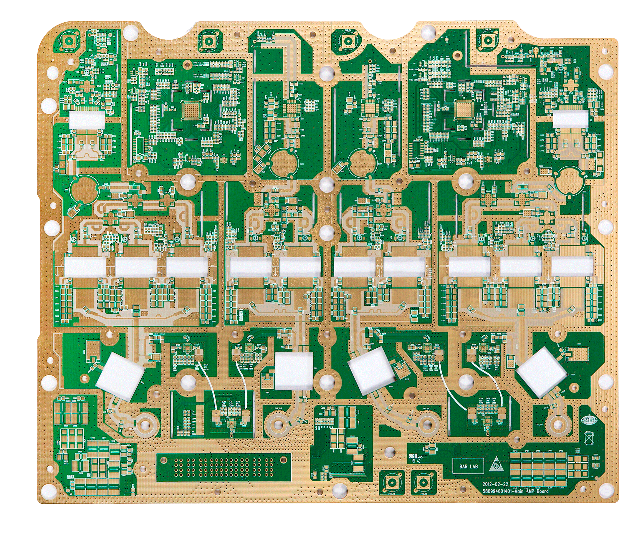
Multilayer RF PCBs contain two or more conductive copper layers separated by insulating dielectric substrates. The multiple layers allow RF designers to route signals horizontally and vertically within the board, enabling greater circuit density and complexity compared to single or double layer boards. In this article, we will examine the key benefits of using multilayer constructions for RF PCB design.
Higher Component Density
One of the primary advantages of multilayer RF PCBs is the ability to incorporate more components and circuitry in a constrained space. With more layers, RF designers can efficiently route traces and signals on different layers without collisions and interference. Components can be placed on both sides of the board by utilizing vias to transition between layers. This higher component density leads to smaller overall board sizes. For space-constrained devices like smartphones, wearables and Internet of Things (IoT) gadgets, a compact multilayer RF PCB is essential.
Shielding and Isolation

Sensitive RF circuits require careful isolation and shielding to prevent interference from noise sources. Multilayer boards facilitate this through the strategic placement of ground planes and power planes between layers containing active circuit traces. The ground planes act as barriers to confine noise to individual sections of the board. Sensitive receive circuitry can also be shielded by surrounding it with ground planes or a Faraday cage construction on multiple layers. Differential signaling further benefits from multilayer isolation between tightly coupled differential pairs.
Integrated Passives
In addition to active components, RF PCBs also incorporate substantial passive components like capacitors and resistors. Multilayer boards allow these passives to be directly integrated into the board itself. Capacitance can be created between two planar electrodes patterned on separate layers. Resistors and inductors can also be constructed through the choice of dielectric materials and copper shapes. Integrated passives reduce the need for discrete passives that take up valuable board space. It also eliminates parasitics associated with the mounting of discrete SMT passives.
Impedance Control
Careful impedance control is critical for maintaining signal integrity in RF PCBs. A multilayer stackup provides more variables that can be tuned to obtain the desired characteristic impedance. Dielectric materials with different permittivities can be selected. Reference planes can also be placed at specific distances to control impedance. Transmission lines can be engineered with wider spaces between layers, allowing lighter dielectrics like PTFE to be used for low permittivity.
Crosstalk Minimization
Electromagnetic coupling between traces in close proximity, known as crosstalk, can impair signal quality in RF PCBs. With judiciously planned spacing and routing, multilayer PCBs can minimize crosstalk. Non-adjacent layers can be used for aggressor and victim traces to increase physical separation. Ground planes in between layers also help block crosstalk between layers. Overall, the extra degrees of freedom facilitate crosstalk reduction.
EMI Shielding
Multilayer designs excel at mitigating EMI emission and susceptibility issues. A key technique is creating continuous shielding around EMI sources and sensitive circuits using ground planes and shields constructed with vias. Components can be compartmentalized into shielded sections that prevent interference at board level. Any gaps or slots in the shielding can be minimized by routing signals through filtered connectors or feedthroughs. This improves the EMI performance of the final product.
Thermal Management
The many layers in an RF PCB provide more options for dissipating heat from active components. Inner layers can be assigned as dedicated thermal planes to spread heat laterally. Vias can then conduct heat between layers and to exterior layers where the heat can be transferred to the environment. Ground and power planes between layers also facilitate thermal conduction. Careful thermal analysis during the design phase is important to avoid hotspots in multilayer RF PCBs.
Design for Manufacturing (DFM)
While multilayer RF PCBs provide many benefits, the design complexity also increases. RF engineers should utilize DFM guidelines and work closely with manufacturers to ensure the design can translate to an actual fabricated board. Key considerations include layer stackup, impedance control, lamination process, mechanical tolerances, and reliability testing. Applying DFM principles will minimize prototyping iterations and avoid fabrication issues.
Conclusion
The increasing demands of modern wireless electronics continue to drive innovations in multilayer RF PCBs. With their advantages in density, shielding, integration, impedance control, and thermal management, multilayer RF PCB technology enables the realization of high-performance and compact RF electronic circuitry. Close collaboration between designers and manufacturers is key to optimizing multilayer RF PCB stackups.
Frequently Asked Questions
What are some key considerations when selecting materials for a multilayer RF PCB?
Some important considerations include: dielectric constant, loss tangent, thermal conductivity, Z-axis CTE, moisture absorption, TGlass, roughness, and lamination temperature. These parameters influence electrical performance, manufacturability, and reliability.
How many layers are typically used in multilayer RF PCBs?
Most designs utilize 4-12 layers, but very complex boards may have 20+ layers. More layers allow higher component density at the cost of increased fabrication difficulty and expense. The number of layers depends on circuit complexity and board thickness constraints.
How are different layers aligned when fabricating a multilayer PCB?
Alignment is achieved through the use of tooling holes that run through the entire PCB stackup. Pins are used to align the layers during lamination. Microvias also aid in interlayer alignment. Maintaining tight registration tolerance is critical.
What are thermal vias used for in multilayer RF PCBs?
Thermal vias help conduct heat between layers and to the board exterior. They are placed strategically under hot components and connected with thermal planes to dissipate heat. Thermal vias should have adequate cross-sectional area to transfer heat.
How are integrated capacitors constructed in multilayer RF PCBs?
Parallel plate capacitors can be formed by patterning copper electrode layers separated by a dielectric. Higher values are achieved with thinner dielectrics, larger plate areas, and high dielectric constant materials. Plate layers should not contain thermals or cutouts.
Leave a Reply