Overview of Microwave PCB Technology
Printed circuit boards (PCBs) designed for microwave frequencies are critical components in a wide range of electronics applications including radar systems, satellite communications, and wireless infrastructure. Microwave PCBs operate at frequencies from 300 MHz up to at least 30 GHz. They require special design considerations to account for transmission line effects, impedance matching, electromagnetic interference, and signal integrity at high frequencies.
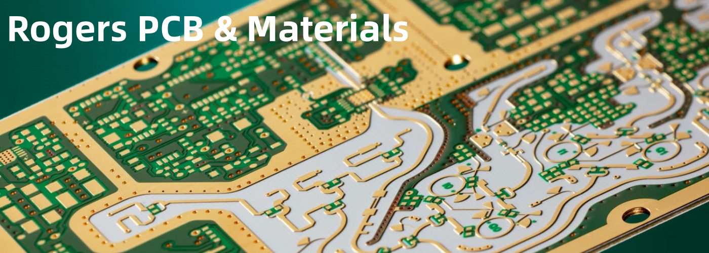
Some key technologies used in microwave PCBs include:
- Microstrip transmission lines – used to route microwave signals along the board. Careful impedance control is needed.
- Striplines – similar to microstrip but with a dielectric above and below the trace. Better isolation and EMI control.
- Buried and blind vias – provides connections between layers while minimizing discontinuities.
- Solid bottom and top copper layers – used for RF shielding and heat dissipation.
- High frequency laminates – materials engineered for stable dielectric constants and low loss. Common materials include PTFE, ceramic filled PTFE, and hydrocarbon ceramics.
- Specialty components – matched impedance resistors, capacitors and transmission lines.
Microwave PCB Design Considerations
Successfully designing and manufacturing a microwave PCB requires attention to parameters such as:
Impedance Control – Trace widths and dielectric materials must be selected to achieve 50 or 75 Ohm controlled impedance transmission lines. This helps avoid reflections and wasted power.
Resonance Control – Careful design of conductor lengths is needed to avoid resonances at the operating frequency or harmonics, which cause ripple and ringing artifacts.
EMI Shielding – At microwave frequencies even small gaps act as antennae for EMI emissions. Extensive ground planes and strategic placement of vias helps isolate sensitive circuits.
Thermal Management – High power microwave circuits require thermal vias, large ground planes, and sometimes on-board heatsinks to dissipate heat.
Material Selection – Dielectric constant tolerance, loss tangent, thermal conductivity and Z-axis CTE are key parameters in choosing the circuit board laminate.
Modeling and Simulation – 3D EM simulation helps verify performance prior to fabrication. This prevents costly re-spins.
Precision Layers – Tight tolerances on trace/space, registration, and consistency help achieve target impedance across designs.
Microwave vs. Traditional PCB Fabrication

Building microwave circuit boards requires special expertise and equipment beyond that used for traditional PCBs operating below 1 GHz. Some key differences include:
- Tighter impedance tolerances are needed – Often ±5% on transmission lines vs. ±10% for traditional PCBs.
- Fabrication usually starts with thermally stable, low loss materials like PTFE or ceramic-filled hydrocarbons. The more common FR-4 is too lossy.
- High frequency dielectrics require tight controls on material thickness and properties. Prepregs are often sliced to tighter thicknesses than used for digital boards.
- Models must account for dielectric constants varying in 3 axes as well as frequency (dispersive effects).
- Smooth copper and low profile surfaces help minimize power loss and reflection. Reverse treated foil and low profile copper are common.
- Plated through holes (PTHs) can cause resonances and reflection above 10 GHz, requiring buried and blind vias instead.
- EMI shielding demands extensive ground planes with close attention to eliminate even small gaps that radiate signals.
- Controlled environment storage and handling procedures prevent moisture absorption which degrades performance.
In summary, microwave PCB fabrication combines high-end materials, tight tolerances, and modeling expertise to yield boards that perform successfully at GHz frequencies.
Key Applications of Microwave PCBs
Microwave PCB technology supports critical functions in sectors like:
- Wireless Infrastructure – Microwave is widely used in 5G networks, backhaul radio links, and other wireless systems. Boards connect power amplifiers, filters, antennas, processors and sensors.
- Radar – Microwave PCBs route signals in phased array antennas, receivers, and radar processors. They must maintain signal integrity and precise timing.
- Satellite – Communication links between satellites and ground stations rely on microwave frequencies. The boards operate in harsh environments.
- Medical – Small microwave systems are used in cancer treatment, imaging, and surgical applications. Reliability is paramount.
- Defense – Radar, electronic warfare, communications and weapons systems depend on microwave circuit boards rated for rugged conditions.
- Test Instrumentation – Boards for oscilloscopes, signal generators, analyzers, and test systems need to function at microwave frequencies with stability.
- Automotive – Short and medium range radar for collision avoidance and autonomous driving use boards operating from 24 GHz to 79 GHz.
Microwave PCB Production Tips
Here are some best practices to follow during the procurement and assembly process to ensure success:
- Select a fabrication shop experienced in building microwave boards, not just standard multilayer PCBs. Ask about tolerances, certifications, and materials.
- Work closely with designers to ensure proper stackup, impedance control, resonance avoidance, and thermal management.
- Share board profiles, models, and requirements with the fab shop early in the design process. Get their feedback.
- Require impedance reports, coupon testing, and rigorous quality assurance testing on completed boards.
- Control moisture exposure which degrades high frequency laminates. Use vacuum sealed bags, dessicant, nitrogen storage.
- Watch for cracked vias around component pads which act as antennas. Use thermally compatible pad shapes and lead-free solder.
- Use assembly shops familiar with soldering large ground planes without bridges, minimizing heat and pressure.
- Perform rigorous RF testing on assembled boards to verify acceptable insertion loss, impedance, and signal transmission.
Following these guidelines helps avoid pitfalls and produces microwave PCBs that perform to their full potential in the final application.
Frequently Asked Questions
Q: What frequency range is considered microwave for PCBs?
A: Microwave PCBs generally operate between 300 MHz to at least 30 GHz, though some speciality boards can function up to 100 GHz. The most common microwave bands used are L (1-2 GHz), S (2-4 GHz), C (4-8 GHz), X (8-12 GHz), Ku (12-18 GHz) and K (18-27 GHz).
Q: Can you use FR-4 and standard PCB processes for microwave frequencies?
A: FR-4 laminate is too lossy for most microwave applications over 1 GHz. The dielectric constant is not tightly controlled and the material exhibits dispersion at higher frequencies. Special microwave laminates and fabrication processes are needed.
Q: What design software is typically used for microwave PCBs?
A: Microwave design relies heavily on 3D electromagnetic (EM) simulation using tools like Ansys HFSS, Keysight ADS and Cadence SiP. This verifies performance prior to fabrication since microwave PCBs are expensive to produce.
Q: How are components mounted on microwave PCBs?
A: Microwave components require precision mounting to match impedances. Soldering is common, along with conductive epoxy. Some boards use wire bonds or ribbons to interconnect MMIC die. Care is taken to minimize parasitic capacitance and inductance.
Q: What testing is used to qualify microwave PCBs?
A: Electrical testing includes insertion loss, return loss, and gain measurements over frequency using network analyzers. Mechanical inspection validates fabrication accuracy. Environment stress screening (ESS) evaluates robustness. Often boards are 100% electrically tested.
Leave a Reply