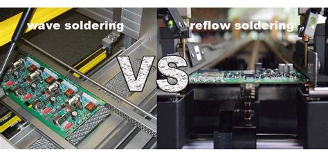
Wave-Reflow Distinction: Understanding the Key Differences
In the world of electronics manufacturing, soldering plays a crucial role in assembling components onto printed circuit boards (PCBs). Two of the most common soldering techniques used in the industry are wave soldering and Reflow Soldering. While both methods aim to create reliable electrical connections, they differ in their processes, applications, and characteristics. In this article, we will explore the distinctions between wave soldering and reflow soldering, helping you understand when to use each technique and how to optimize your manufacturing process.
Table of Contents
- Introduction to Soldering
- Wave Soldering
- Process Overview
- Advantages and Disadvantages
- Suitable Components and PCBs
- Reflow Soldering
- Process Overview
- Advantages and Disadvantages
- Suitable Components and PCBs
- Key Differences Between Wave and Reflow Soldering
- Process Comparison
- Component Compatibility
- PCB Design Considerations
- Cost and Efficiency
- Choosing the Right Soldering Method
- Factors to Consider
- Decision Matrix
- Case Studies
- Optimizing Your Soldering Process
- Best Practices for Wave Soldering
- Best Practices for Reflow Soldering
- Quality Control and Inspection
- Frequently Asked Questions (FAQ)
- Conclusion
1. Introduction to Soldering
Soldering is a process that joins two or more metal items by melting and applying a filler metal (solder) into the joint, creating a strong electrical and mechanical bond. In electronics manufacturing, soldering is used to attach components to PCBs, ensuring proper functionality and reliability. The two most common soldering methods are wave soldering and reflow soldering.

2. Wave Soldering
Process Overview
Wave soldering is a bulk soldering process that involves passing a PCB over a molten solder wave. The process follows these steps:
1. PCB preparation: Components are inserted into the PCB, and the board is placed on a conveyor.
2. Flux application: A thin layer of flux is applied to the bottom of the PCB to remove oxides and improve solder wettability.
3. Preheating: The PCB is preheated to activate the flux and minimize thermal shock.
4. Solder wave contact: The PCB passes over a molten solder wave, which wets the exposed component leads and PCB pads.
5. Cooling: The PCB cools, allowing the solder to solidify and form strong joints.
Advantages and Disadvantages
Advantages of wave soldering:
– High throughput and efficiency for large-scale production
– Suitable for both through-hole and surface mount components
– Ideal for complex PCBs with high component density
– Provides good mechanical strength and reliability
Disadvantages of wave soldering:
– Limited control over individual solder joints
– Potential for bridging and solder defects
– Requires careful PCB design and component placement
– Not suitable for heat-sensitive components
Suitable Components and PCBs
Wave soldering is commonly used for:
– Through-hole components
– Large, heavy components
– Components with leads on the bottom side of the PCB
– Double-sided PCBs with a mix of through-hole and surface mount components

3. Reflow Soldering
Process Overview
Reflow soldering is a process that uses a controlled heat profile to melt and solidify solder paste, creating a bond between surface mount components and PCB pads. The process involves the following steps:
1. Solder paste application: Solder paste, a mixture of powdered solder and flux, is applied to the PCB pads using stencil printing or dispensing.
2. Component placement: Surface mount components are placed onto the solder paste deposits using Pick-and-Place machines or manual methods.
3. Reflow: The PCB passes through a reflow oven, following a predetermined temperature profile that melts the solder paste, allowing it to wet the component leads and PCB pads.
4. Cooling: The PCB cools, allowing the solder to solidify and form strong joints.
Advantages and Disadvantages
Advantages of reflow soldering:
– Precise control over solder joint formation
– High repeatability and consistency
– Suitable for high-density PCBs with small components
– Faster process compared to wave soldering for surface mount components
Disadvantages of reflow soldering:
– Limited to surface mount components
– Requires careful control of the reflow profile to avoid component damage
– Solder paste application can be challenging for fine-pitch components
– Higher initial equipment costs compared to wave soldering
Suitable Components and PCBs
Reflow soldering is primarily used for:
– Surface mount components
– Fine-pitch components
– PCBs with high component density
– Single-sided or double-sided PCBs with surface mount components only

4. Key Differences Between Wave and Reflow Soldering
Process Comparison
| Aspect | Wave Soldering | Reflow Soldering |
|---|---|---|
| Solder application | Molten solder wave | Solder paste |
| Component types | Through-hole and surface mount | Surface mount only |
| PCB passage | Conveyor over solder wave | Reflow oven |
| Process control | Limited individual joint control | Precise profile control |
| Throughput | High for mixed component PCBs | High for surface mount PCBs |
Component Compatibility
Wave soldering is suitable for both through-hole and surface mount components, while reflow soldering is limited to surface mount components. When choosing between the two methods, consider the types of components used on your PCB and their packaging.
PCB Design Considerations
PCB design plays a crucial role in the success of both wave and reflow soldering processes. For wave soldering, ensure proper component placement, orientation, and lead spacing to minimize solder defects. In reflow soldering, pay attention to solder mask design, pad sizes, and thermal considerations to achieve optimal results.
Cost and Efficiency
The cost and efficiency of wave and reflow soldering depend on various factors, such as production volume, component mix, and PCB complexity. Wave soldering is generally more cost-effective for high-volume production of mixed component PCBs, while reflow soldering is more efficient for high-density surface mount PCBs.
5. Choosing the Right Soldering Method
Factors to Consider
When deciding between wave soldering and reflow soldering, consider the following factors:
– Component types and packaging
– PCB design and complexity
– Production volume and scalability
– Available equipment and resources
– Quality and reliability requirements
– Cost and efficiency targets
Decision Matrix
Use a decision matrix to systematically evaluate the suitability of wave soldering and reflow soldering for your specific project. Assign weights to each factor based on their importance and score each soldering method accordingly. The method with the highest total score is likely the most appropriate choice.
Case Studies
Analyze case studies of successful projects that utilized wave soldering or reflow soldering. Learn from their experiences, challenges, and best practices to inform your own decision-making process.
6. Optimizing Your Soldering Process
Best Practices for Wave Soldering
- Ensure proper PCB design and component placement
- Maintain optimal solder wave height and temperature
- Use appropriate flux and preheating settings
- Implement regular maintenance and calibration of equipment
- Monitor and control the solder bath composition
Best Practices for Reflow Soldering
- Use high-quality solder paste with the correct particle size and alloy composition
- Ensure accurate solder paste printing or dispensing
- Optimize the reflow profile for your specific components and PCB
- Implement proper component placement and orientation
- Conduct regular maintenance and calibration of reflow ovens
Quality Control and Inspection
Regardless of the soldering method used, implementing a robust quality control and inspection process is essential. Conduct visual inspections, automated optical inspections (AOI), and Electrical Testing to identify and rectify any soldering defects or issues.
7. Frequently Asked Questions (FAQ)
-
Q: Can wave soldering be used for surface mount components?
A: Yes, wave soldering can be used for surface mount components, but it requires careful PCB design and component placement to ensure proper solder joint formation and avoid defects. -
Q: Is reflow soldering suitable for through-hole components?
A: Reflow soldering is not recommended for through-hole components, as the solder paste may not flow properly into the component holes, leading to weak or incomplete solder joints. -
Q: How can I minimize solder bridging in wave soldering?
A: To minimize solder bridging in wave soldering, ensure proper component spacing, use an appropriate solder mask, and optimize the solder wave height and conveyor speed. -
Q: What is the purpose of flux in soldering processes?
A: Flux is used in soldering processes to remove oxides from the metal surfaces, promote solder wettability, and protect the joint from oxidation during the soldering process. -
Q: How do I choose the right solder alloy for my application?
A: When choosing a solder alloy, consider factors such as melting temperature, mechanical strength, electrical conductivity, and compatibility with your components and PCB materials. Consult solder manufacturers or industry standards for guidance.
8. Conclusion
Understanding the differences between wave soldering and reflow soldering is crucial for optimizing your electronics manufacturing process. By considering the key factors, such as component compatibility, PCB design, cost, and efficiency, you can make an informed decision on the most suitable soldering method for your project.
Implementing best practices and conducting thorough quality control and inspection will help ensure the reliability and performance of your soldered assemblies. Continuously monitor and improve your soldering processes to stay competitive in the ever-evolving electronics industry.
Leave a Reply