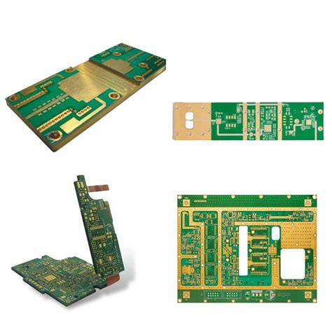
Introduction to HDI PCB
High Density Interconnect (HDI) PCBs are printed circuit boards with higher wiring density per unit area compared to conventional PCBs. HDI PCBs have finer lines and spaces (<100 μm), smaller vias (<150 μm), and capture pads (<400 μm), and higher connection pad density (>20 pads/cm2) than traditional PCBs.
HDI PCB technology is driven by the need for miniaturization in electronics to create smaller, lighter, faster devices with more functionality. HDI allows for higher component density and improved electrical performance in a smaller form factor. Smartphones, tablets, laptops, wearables, medical devices, and aerospace/defense systems commonly use HDI PCB designs.
Benefits and Advantages of HDI PCB
The main benefits and advantages of HDI PCBs include:
-
Miniaturization: HDI allows designers to pack more functionality into a smaller footprint. Smaller electronic devices are more portable and lightweight.
-
Higher interconnect density: Finer traces, smaller vias and capture pads, and higher connection pad density enable more interconnections between components.
-
Improved electrical performance: Shorter signal paths reduce impedance, crosstalk, and propagation delay. Power and ground planes provide better power distribution and reduce EMI/RFI.
-
Reduced layer count: HDI techniques like blind/Buried vias and microvias allow for more interconnections on fewer layers, reducing overall board thickness.
-
Cost reduction: Although HDI PCBs have a higher cost per unit area, the overall cost can be lower by reducing the PCB size and layer count compared to a conventional design.
-
Improved reliability: HDI PCBs have smaller plated Through-holes and vias which undergo less thermo-mechanical stress during fabrication and operation, improving reliability.

HDI PCB Construction and Manufacturing
HDI PCBs are classified into three types based on the density and manufacturing complexity:
| HDI Type | Density | Features |
|---|---|---|
| Type 1 | Moderate | Blind/buried vias, up to 2 lamination cycles |
| Type 2 | High | Blind/buried vias, up to 4 lamination cycles |
| Type 3 | Very High | Blind/buried vias, up to 6 lamination cycles, coreless construction |
HDI PCBs are constructed using a sequential lamination process that builds up the layers with microvias and conductors. The process involves:
- Drilling and plating through-holes on the base core
- Patterning and etching conductors on the base core
- Laminating prepreg and copper foils to the base core
- Laser drilling blind/buried microvias
- Depositing copper to form the interconnections
- Repeating steps 3-5 to build up additional layers
- Patterning and etching conductors on the outer layers
- Applying Solder Mask and surface finish
Laser drilling is used to create blind and buried microvias with diameters down to 50 μm. The microvias are filled with electroplated copper to form the interconnections between layers. Stacked, staggered, and stacked-and-staggered microvia configurations are used to connect multiple layers.

HDI PCB Design Considerations and Guidelines
Designing HDI PCBs requires careful consideration of the electrical, mechanical, and manufacturing requirements. Key design considerations and guidelines include:
-
Stack-up design: The stack-up should be symmetrical and balanced to prevent warpage. Use high-Tg, low-CTE materials to minimize thermo-mechanical stress.
-
Microvia design: Follow the manufacturer’s guidelines for microvia diameter, pitch, and fill requirements. Avoid stacked microvias if possible to improve manufacturing yield.
-
Trace width/spacing: Use the finest trace width/spacing that can be reliably manufactured. Avoid sharp corners and use teardrop pads to improve mechanical strength.
-
Impedance control: Use controlled impedance traces for high-speed signals. Perform signal integrity simulations to optimize the trace geometry and spacing.
-
Power distribution: Use separate power and ground planes for different voltage rails. Provide adequate decoupling capacitors near ICs to reduce power supply noise.
-
EMI/RFI suppression: Use guard rings, stitching vias, and ground planes to reduce electromagnetic and radio frequency interference. Follow high-speed digital design guidelines.
-
Thermal management: Use thermal vias and heatsinks to dissipate heat from high-power components. Avoid placing heat-sensitive components near hot components.
-
DFM: Follow design for manufacturing (DFM) guidelines to ensure the HDI PCB can be reliably manufactured. Perform DRC/DFM checks before sending the design for fabrication.

HDI PCB Applications and Industries
HDI PCBs are used in a wide range of applications and industries that require high performance, miniaturization, and reliability. Some of the key applications and industries include:
-
Consumer electronics: Smartphones, tablets, laptops, digital cameras, gaming consoles, VR/AR devices.
-
Telecommunications: 5G infrastructure, base stations, routers, switches, fiber-optic equipment.
-
Automotive: Advanced driver assistance systems (ADAS), infotainment systems, electric vehicles, autonomous vehicles.
-
Medical devices: Implantable devices, wearable health monitors, surgical instruments, diagnostic equipment.
-
Aerospace/Defense: Satellites, avionics, radar systems, missile guidance, soldier systems.
-
Industrial: Factory automation, process control, robotics, IoT sensors and gateways.
As electronic devices continue to advance in performance and shrink in size, the demand for HDI PCBs will continue to grow across these industries.
HDI PCB Market Trends and Future Outlook
The global HDI PCB market was valued at USD 10.3 billion in 2020 and is projected to reach USD 22.4 billion by 2026, at a CAGR of 13.8% during the forecast period (2021-2026).
The growth of the HDI PCB market is driven by several key trends:
-
5G adoption: The rollout of 5G networks and devices is driving demand for HDI PCBs in telecommunications infrastructure and 5G smartphones.
-
IoT proliferation: The growth of the Internet of Things (IoT) is creating demand for small, low-power, wireless-connected devices that require HDI PCBs.
-
Automotive electronics: The increasing adoption of ADAS, infotainment systems, and electric vehicles is driving demand for HDI PCBs in the automotive industry.
-
Wearable devices: The popularity of smartwatches, fitness trackers, and other wearable devices is driving demand for HDI flexible and Rigid-Flex PCBs.
-
Advanced packaging: The adoption of advanced IC packaging techniques like 2.5D/3D, fan-out wafer-level packaging (FOWLP) is driving demand for advanced HDI substrates.
The Asia-Pacific region dominates the HDI PCB market due to the presence of major electronics manufacturers and consumers in countries like China, South Korea, Taiwan, and Japan. North America and Europe are also significant markets for HDI PCBs in the aerospace/defense, automotive, and medical device industries.
As electronic devices continue to push the boundaries of performance and miniaturization, HDI PCB technology will continue to advance to meet the increasing demands of the electronics industry. Innovations in materials, manufacturing processes, and design tools will enable even higher density and more complex HDI PCBs in the future.
Frequently Asked Questions (FAQ)
1. What is the difference between HDI PCB and conventional PCB?
HDI PCBs have higher wiring density per unit area compared to conventional PCBs. They have finer lines and spaces (<100 μm), smaller vias (<150 μm), and capture pads (<400 μm), and higher connection pad density (>20 pads/cm2) than traditional PCBs. HDI PCBs enable higher component density, improved electrical performance, and miniaturization compared to conventional PCBs.
2. What are the types of HDI PCBs?
HDI PCBs are classified into three types based on the density and manufacturing complexity:
– Type 1: Moderate density, blind/buried vias, up to 2 lamination cycles
– Type 2: High density, blind/buried vias, up to 4 lamination cycles
– Type 3: Very high density, blind/buried vias, up to 6 lamination cycles, coreless construction
3. What are the key benefits of using HDI PCBs?
The key benefits of using HDI PCBs include:
– Miniaturization: Smaller form factor and higher component density
– Improved electrical performance: Shorter signal paths, reduced noise and crosstalk
– Reduced layer count: More interconnections on fewer layers
– Cost reduction: Lower overall cost due to smaller PCB size and layer count
– Improved reliability: Smaller vias undergo less thermo-mechanical stress
4. What are the main applications and industries for HDI PCBs?
HDI PCBs are used in a wide range of applications and industries, including:
– Consumer electronics: Smartphones, tablets, laptops, wearables
– Telecommunications: 5G infrastructure, routers, switches
– Automotive: ADAS, infotainment systems, electric vehicles
– Medical devices: Implantable devices, wearable health monitors
– Aerospace/Defense: Satellites, avionics, radar systems
– Industrial: Factory automation, robotics, IoT sensors
5. What are the key design considerations for HDI PCBs?
The key design considerations for HDI PCBs include:
– Stack-up design: Symmetrical and balanced, high-Tg low-CTE materials
– Microvia design: Follow manufacturer’s guidelines for diameter, pitch, and fill
– Trace width/spacing: Use finest manufacturable traces, avoid sharp corners
– Impedance control: Use controlled impedance for high-speed signals
– Power distribution: Use power/ground planes, adequate decoupling
– EMI/RFI suppression: Use guard rings, stitching vias, ground planes
– Thermal management: Use thermal vias and heatsinks for high-power components
– DFM: Follow design for manufacturing guidelines, perform DRC/DFM checks
Conclusion
HDI PCB technology is enabling the next generation of electronic devices with higher performance, smaller form factors, and greater functionality. By pushing the boundaries of PCB density and miniaturization, HDI PCBs are meeting the demands of a wide range of industries and applications, from consumer electronics to aerospace and defense.
As the electronics industry continues to evolve and innovate, HDI PCB technology will play an increasingly critical role in enabling new products and capabilities. With advances in materials, manufacturing processes, and design tools, HDI PCBs will continue to get smaller, denser, and more complex in the future.
For designers and engineers, understanding the benefits, challenges, and design considerations of HDI PCBs is essential for creating successful products in today’s competitive electronics marketplace. By following best practices and staying up-to-date with the latest HDI PCB technologies and trends, designers can unlock the full potential of this powerful technology and create innovative electronic devices that meet the needs of consumers and businesses alike.
Leave a Reply