What is Laser Direct Imaging?
Laser Direct Imaging (LDI) is an advanced PCB fabrication process where a laser beam directly transfers the circuit pattern onto the photoresist layer of the PCB, eliminating the need for traditional photomasks. This state-of-the-art technology offers numerous advantages over conventional photolithography methods, including higher precision, faster processing times, and improved flexibility in circuit design.
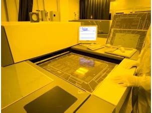
How Does Laser Direct Imaging Work?
In the LDI process, a high-powered laser beam is used to selectively expose the photoresist layer on the PCB. The laser is controlled by a computer-aided design (CAD) file that contains the circuit pattern information. As the laser beam scans across the surface of the photoresist, it activates the areas that will form the conductive traces on the PCB.
The key components of an LDI system include:
- Laser source: A high-powered laser, typically ultraviolet (UV) or visible light, is used to expose the photoresist.
- Optical system: A series of lenses and mirrors are used to focus and direct the laser beam onto the PCB surface.
- Scanning system: A precise positioning system moves the laser beam or the PCB to ensure accurate exposure of the circuit pattern.
- Computer control: A CAD file containing the circuit pattern information is used to control the laser and scanning systems.
After exposure, the PCB undergoes a development process to remove the exposed photoresist, revealing the desired circuit pattern. The remaining photoresist acts as a protective mask during the subsequent etching process, which removes the unwanted copper, leaving only the conductive traces.
Advantages of Laser Direct Imaging
Compared to traditional photolithography methods, LDI offers several significant advantages:
- Higher precision: LDI can achieve finer feature sizes and more accurate positioning, enabling the fabrication of high-density PCBs with smaller trace widths and spacing.
- Faster processing times: By eliminating the need for photomasks, LDI reduces the number of process steps and allows for faster setup and exposure times.
- Improved flexibility: LDI enables quick and easy changes to circuit designs, as modifications can be made directly in the CAD file without the need to create new photomasks.
- Reduced costs: The elimination of photomasks and the associated storage and maintenance costs can lead to significant cost savings, particularly for low-volume or prototype production.
- Enhanced yield: LDI’s high precision and direct imaging capabilities reduce the risk of defects and improve overall PCB yield.
Applications of Laser Direct Imaging
LDI technology is particularly well-suited for applications that require high-density PCBs, fine feature sizes, and rapid prototyping. Some of the key applications include:
- High-density interconnect (HDI) PCBs: LDI enables the fabrication of HDI PCBs with fine pitch traces and micro-vias, which are essential for advanced electronics packaging.
- Aerospace and defense: The high reliability and precision of LDI make it ideal for producing PCBs for critical aerospace and defense applications.
- Medical devices: LDI’s ability to produce high-density, miniaturized PCBs is valuable for the development of advanced medical devices and implantable electronics.
- Automotive electronics: As vehicles incorporate more electronic systems, LDI helps meet the demand for compact, high-performance PCBs in automotive applications.
- Consumer electronics: LDI’s flexibility and rapid prototyping capabilities are beneficial for the fast-paced consumer electronics industry, where product life cycles are short and time-to-market is critical.

RAYPCB’s Expertise in Laser Direct Imaging
RAYPCB, a leading PCB fabrication company, has extensive experience in utilizing LDI technology to produce high-quality, high-density PCBs for a wide range of industries. With state-of-the-art LDI equipment and a team of skilled professionals, RAYPCB can deliver PCBs with the following specifications:
| Feature | Specification |
|---|---|
| Minimum trace width/spacing | 50 μm / 50 μm |
| Minimum via diameter | 100 μm |
| Minimum via-to-via spacing | 200 μm |
| Minimum via-to-trace spacing | 100 μm |
| Maximum aspect ratio | 10:1 |
| Maximum layer count | 20+ |
RAYPCB’s LDI capabilities enable the company to serve customers in various industries, including aerospace, defense, medical, automotive, and consumer electronics. By continuously investing in the latest LDI technology and training its staff, RAYPCB ensures that it can meet the evolving needs of its customers and deliver high-quality PCBs with quick turnaround times.

The Future of Laser Direct Imaging
As the demand for high-density, high-performance PCBs continues to grow, LDI technology is expected to play an increasingly important role in PCB fabrication. Advancements in laser technology, such as the development of shorter wavelength lasers and improved beam control, will enable even finer feature sizes and higher precision.
Additionally, the integration of LDI with other advanced manufacturing technologies, such as 3D printing and embedded components, will open up new possibilities for PCB design and functionality. As a result, LDI is likely to become the standard for high-end PCB fabrication in the coming years.

Frequently Asked Questions (FAQ)
- What is the main difference between LDI and traditional photolithography?
-
LDI uses a laser to directly transfer the circuit pattern onto the photoresist, while traditional photolithography uses a photomask to selectively expose the photoresist to UV light.
-
What are the key benefits of using LDI in PCB fabrication?
-
LDI offers higher precision, faster processing times, improved flexibility in circuit design, reduced costs, and enhanced yield compared to traditional photolithography methods.
-
What industries commonly use PCBs fabricated with LDI technology?
-
Industries that commonly use PCBs fabricated with LDI include aerospace, defense, medical devices, automotive electronics, and consumer electronics.
-
How does RAYPCB ensure the quality of its LDI-fabricated PCBs?
-
RAYPCB invests in state-of-the-art LDI equipment, trains its staff in the latest techniques, and implements strict quality control measures to ensure the high quality of its LDI-fabricated PCBs.
-
What advancements can we expect in LDI technology in the future?
- Future advancements in LDI technology may include the development of shorter wavelength lasers for finer feature sizes, improved beam control for higher precision, and integration with other advanced manufacturing technologies like 3D printing and embedded components.
In conclusion, Laser Direct Imaging is a cutting-edge technology that is revolutionizing PCB fabrication by offering higher precision, faster processing times, and improved flexibility compared to traditional methods. As a leading PCB fabrication company, RAYPCB has embraced LDI technology to deliver high-quality, high-density PCBs for a wide range of industries. With ongoing advancements in laser technology and the increasing demand for high-performance PCBs, LDI is poised to become the standard for high-end PCB fabrication in the years to come.
Leave a Reply