Understanding PCB Stackups
A PCB stackup refers to the arrangement of layers within a printed circuit board, including the copper layers, insulating layers, and other materials used in the construction of the board. The stackup plays a critical role in determining the electrical, mechanical, and thermal properties of the PCB, as well as its overall performance and reliability.
Importance of PCB Stackups
A well-designed PCB stackup is essential for several reasons:
-
Signal Integrity: The arrangement of layers in a PCB can significantly impact the signal integrity of the board. Proper layer stacking helps minimize crosstalk, reduce electromagnetic interference (EMI), and ensure clean and stable signal transmission.
-
Impedance Control: The stackup configuration directly affects the characteristic impedance of the PCB traces. By carefully selecting the layer arrangement and dielectric materials, designers can achieve the desired impedance values for various applications, such as high-speed digital circuits or RF systems.
-
Thermal Management: The choice of materials and their placement within the stackup can influence the thermal dissipation properties of the PCB. Effective thermal management is crucial for preventing overheating and ensuring the long-term reliability of the board and its components.
-
Manufacturing Feasibility: The stackup design must take into account the manufacturability of the PCB. Factors such as the number of layers, material compatibility, and drilling requirements can impact the ease and cost of fabrication.
RAYPCB’s Updated Standard Stackup for Multi-layer PCBs
RAYPCB has introduced several updates to its standard stackup for multi-layer PCBs to address the evolving needs of the electronics industry. These updates aim to enhance signal integrity, improve thermal management, and optimize manufacturing processes.
Key Updates in RAYPCB’s Standard Stackup
-
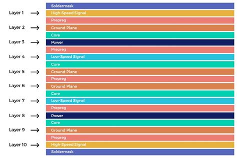
Increased Layer Count Options: RAYPCB now offers a wider range of layer count options for its standard stackup, catering to the growing complexity of modern PCB designs. Customers can choose from 4, 6, 8, 10, 12, 14, 16, 18, and 20-layer configurations, providing greater flexibility in design and functionality.
-
Enhanced Material Selection: The updated stackup incorporates a carefully curated selection of high-performance materials, including low-loss and high-speed laminates, to meet the demands of advanced applications. These materials offer superior electrical properties, such as lower dielectric constants and dissipation factors, which are essential for maintaining signal integrity in high-frequency circuits.
-
Optimized Impedance Control: RAYPCB has refined its stackup configuration to provide better control over impedance values. By strategically positioning signal layers and adjusting the thickness of dielectric materials, the updated stackup ensures more accurate and consistent impedance matching across the board.
-
Improved Thermal Management: The new standard stackup incorporates dedicated thermal management layers, such as thick copper planes or specialized heat-spreading materials, to enhance the PCB’s ability to dissipate heat effectively. This improvement is particularly valuable for power-intensive applications or high-density designs that generate significant amounts of heat.
-
Streamlined Manufacturing Process: RAYPCB has optimized its manufacturing processes to accommodate the updated standard stackup efficiently. The company has invested in advanced equipment and training to ensure consistent quality and faster turnaround times for multi-layer PCB production.
Benefits of RAYPCB’s Updated Standard Stackup
The updates made by RAYPCB to its standard stackup for multi-layer PCBs offer several benefits to designers, engineers, and manufacturers:
-
Enhanced Performance: The improved signal integrity, impedance control, and thermal management properties of the updated stackup contribute to better overall performance of the PCB. This enhancement translates to more reliable and efficient electronic devices and systems.
-
Increased Design Flexibility: With a wider range of layer count options and high-performance materials, designers have greater flexibility in creating complex and feature-rich PCBs. The updated stackup accommodates a broader spectrum of applications, from high-speed digital circuits to RF and mixed-signal designs.
-
Cost-effectiveness: RAYPCB’s streamlined manufacturing process for the updated standard stackup helps reduce production costs and lead times. By offering a well-defined and optimized stackup configuration, RAYPCB minimizes the need for custom stackups, which can be more expensive and time-consuming to fabricate.
-
Reduced Time-to-Market: The combination of enhanced performance, increased design flexibility, and streamlined manufacturing enables faster product development cycles. Designers and manufacturers can bring their products to market more quickly, gaining a competitive edge in the fast-paced electronics industry.

Designing with RAYPCB’s Updated Standard Stackup
To fully leverage the benefits of RAYPCB’s updated standard stackup, designers should consider the following guidelines when creating their multi-layer PCB layouts:
-
Layer Assignment: Carefully assign signals to the appropriate layers based on their requirements for signal integrity, impedance control, and routing density. Follow RAYPCB’s recommendations for layer arrangement to ensure optimal performance.
-
Material Selection: Choose the appropriate laminate materials from RAYPCB’s updated selection based on the electrical, thermal, and mechanical requirements of your application. Consider factors such as dielectric constant, dissipation factor, and thermal conductivity when making your choice.
-
Impedance Calculation: Use RAYPCB’s provided impedance calculation tools or consult with their technical support team to determine the appropriate trace widths and spacing for your desired impedance values. Accurate impedance control is crucial for maintaining signal integrity and minimizing reflections.
-
Thermal Management: Incorporate thermal management techniques, such as the use of dedicated thermal layers or the placement of thermal vias, to ensure efficient heat dissipation. Follow RAYPCB’s guidelines for thermal layer placement and design to maximize the effectiveness of the updated stackup.
-
Design Rule Compliance: Adhere to RAYPCB’s design rules and guidelines for the updated standard stackup. This includes minimum trace widths, spacing requirements, drill sizes, and other manufacturing constraints. Compliance with these rules ensures the manufacturability and reliability of your PCB.

Frequently Asked Questions (FAQ)
-
Q: What is the maximum number of layers supported in RAYPCB’s updated standard stackup?
A: RAYPCB’s updated standard stackup supports up to 20 layers for multi-layer PCBs. -
Q: Can I still use custom stackups with RAYPCB?
A: Yes, RAYPCB continues to offer custom stackup options for specific requirements that cannot be met by the standard stackup. However, custom stackups may have longer lead times and higher costs compared to the standard stackup. -
Q: How does the updated stackup improve signal integrity?
A: The updated stackup incorporates high-performance materials with lower dielectric constants and dissipation factors, which help reduce signal loss and maintain signal integrity. Additionally, the optimized layer arrangement and impedance control measures minimize crosstalk and reflections. -
Q: What thermal management options are available in the updated standard stackup?
A: RAYPCB’s updated standard stackup includes dedicated thermal management layers, such as thick copper planes or specialized heat-spreading materials, to enhance heat dissipation. Designers can also incorporate thermal vias and other thermal management techniques in their PCB layout. -
Q: How can I ensure my design is compatible with RAYPCB’s updated standard stackup?
A: To ensure compatibility, follow RAYPCB’s design guidelines and recommendations for layer assignment, material selection, impedance calculation, and thermal management. Adhere to the provided design rules and consult with RAYPCB’s technical support team for any specific questions or concerns.

Conclusion
RAYPCB’s updated standard stackup for multi-layer PCBs represents a significant advancement in PCB manufacturing technology. By offering enhanced signal integrity, improved thermal management, and increased design flexibility, the updated stackup empowers designers and engineers to create high-performance, reliable, and cost-effective PCBs for a wide range of applications.
As the electronics industry continues to evolve, with faster data rates, higher frequencies, and more complex designs, the importance of a well-designed PCB stackup cannot be overstated. RAYPCB’s commitment to staying at the forefront of PCB manufacturing technology ensures that its customers have access to the latest advancements and best practices in PCB fabrication.
By leveraging RAYPCB’s updated standard stackup and following the recommended design guidelines, designers and manufacturers can unlock the full potential of their multi-layer PCBs, ultimately leading to better products, shorter time-to-market, and increased competitiveness in the dynamic world of electronics.
| Layer | Material | Thickness (mm) | Description |
|---|---|---|---|
| Top Copper | Copper | 0.035 | Signal layer |
| Prepreg | FR-4 | 0.180 | Dielectric layer |
| Inner Copper 1 | Copper | 0.035 | Signal layer |
| Core | FR-4 | 0.200 | Dielectric layer |
| Inner Copper 2 | Copper | 0.035 | Signal layer |
| Prepreg | FR-4 | 0.180 | Dielectric layer |
| Bottom Copper | Copper | 0.035 | Signal layer |
Table 1: Example 4-layer PCB stackup using RAYPCB’s updated standard materials and thicknesses.
| Layer Count | Standard Thickness (mm) | Typical Applications |
|---|---|---|
| 4 | 0.8 – 1.6 | Simple digital circuits, low-speed designs |
| 6 | 1.2 – 2.0 | Digital and mixed-signal designs, moderate-speed applications |
| 8 | 1.6 – 2.4 | Complex digital designs, high-speed applications |
| 10 | 2.0 – 3.2 | High-speed digital, RF, and mixed-signal designs |
| 12+ | 2.4 – 4.0+ | Very high-speed, high-density, and advanced packaging applications |
Table 2: RAYPCB’s updated standard stackup options for various layer counts and typical applications.
Leave a Reply