
RF & Microwave Blog
-
Via in Pad Callout VIPPO
Posted by
–
Read more: Via in Pad Callout VIPPOWhat is Via in Pad Callout (VIPPO)? Via in Pad Callout, or VIPPO, is a PCB design technique that involves placing vias directly inside the surface mount pads of components. This technique is becoming increasingly popular in high-density PCB designs as it allows for more efficient use of board space […]
-
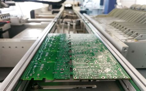 Read more: Explaining Reflow Soldering for PCB Assembly by RAYPCB
What is Reflow Soldering? Reflow soldering is a process used in printed circuit board (PCB) assembly to attach surface mount components to the board. It involves applying solder paste, a mixture of tiny solder particles and flux, to the pads on the PCB. The components are then placed onto the […]
-
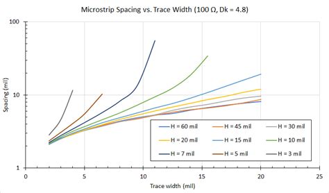
How to Calculate the PCB Trace Impedance
Posted by
–
 Read more: How to Calculate the PCB Trace Impedance
Introduction to PCB Trace Impedance Printed Circuit Board (PCB) trace impedance is a crucial factor in the design and performance of high-speed electronic circuits. It is essential to maintain the proper impedance of the traces to ensure signal integrity, minimize reflections, and reduce electromagnetic interference (EMI). In this comprehensive guide, […]
-
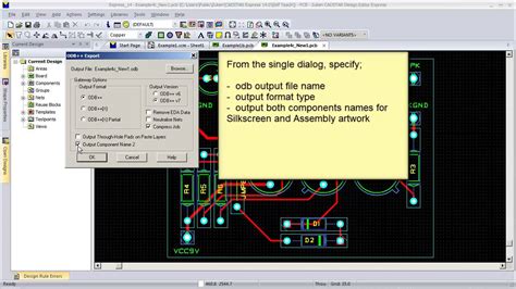
CADSTAR for layout professionals
Posted by
–
 Read more: CADSTAR for layout professionals
What is CADSTAR? CADSTAR is a PCB Design software developed by Zuken, a leading provider of electrical and electronic design automation solutions. The software offers a complete set of tools for designing and documenting PCB Layouts, from schematic capture to final manufacturing output. CADSTAR is known for its user-friendly interface, […]
-
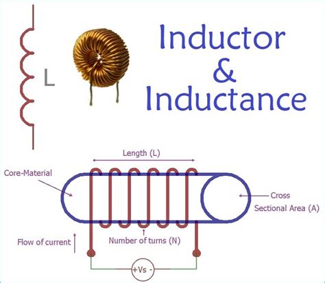
How to Calculate the Inductance of PCB Trace
Posted by
–
 Read more: How to Calculate the Inductance of PCB Trace
Introduction to PCB Inductance Printed Circuit Board (PCB) inductance is a crucial factor in the design and performance of high-speed electronic circuits. Inductance is the property of a conductor that opposes changes in current flow, resulting in the storage of magnetic energy. In PCBs, traces act as inductors, and their […]
-
PCB Trace to Plane Capacitance Formula
Posted by
–
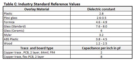 Read more: PCB Trace to Plane Capacitance Formula
Introduction to PCB Capacitance Printed Circuit Boards (PCBs) are essential components in modern electronics, providing a platform for interconnecting various electronic components. One crucial aspect of PCB Design is understanding and managing the capacitance between traces and planes. This article delves into the concept of PCB trace to plane capacitance, […]
-
 Read more: Differential trace impedance without reference plane
Introduction to Differential Trace Impedance Differential trace impedance is a crucial factor in the design of high-speed digital circuits, especially in applications where signal integrity and electromagnetic compatibility (EMC) are of utmost importance. In a differential signaling system, two conductors carry complementary signals, which are equal in magnitude but opposite […]
-
 Read more: Immersion Silver and Other Lead Free PCB Surfaces
Introduction to Lead-Free PCB Surfaces The electronics industry has been moving towards lead-free PCB surfaces for many years now, driven by environmental and health concerns associated with lead. Lead-free PCB surfaces offer several advantages, including improved reliability, better thermal stability, and enhanced electrical performance. In this article, we will explore […]
-
PCB manufacturer in Vietnam
Posted by
–
 Read more: PCB manufacturer in Vietnam
Introduction to PCB Manufacturing in Vietnam Vietnam has emerged as a prominent player in the global electronics manufacturing industry, particularly in the production of printed circuit boards (PCBs). The country’s growth in this sector can be attributed to its skilled workforce, competitive labor costs, and favorable government policies that attract […]
-
Ultraviolet Lasers In PCB Manufacturing
Posted by
–
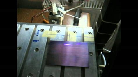 Read more: Ultraviolet Lasers In PCB Manufacturing
Introduction to PCB UV-Lasers Printed Circuit Boards (PCBs) are the backbone of modern electronics, found in everything from smartphones to aerospace systems. The manufacturing process of PCBs has evolved significantly over the years, with new technologies constantly emerging to improve efficiency, precision, and reliability. One such technology that has gained […]
Recent Posts
- How to Select Material for Your PCBs from Cost and Reliability Considerations
- Problems of EMC Technology Application in PCB Design of Electronic Devices and the Strategies
- Fabrication Technology on Flex-Rigid PCB Window
- Problems of High-Frequency and High-Speed Multilayer PCB Fabrication and Their Solutions
- Key Difficulties and Tips for Backplane PCB Fabrication