Introduction to BGA Assembly
Ball Grid Array (BGA) is a surface-mount packaging used for integrated circuits. BGA packages are used to permanently mount devices such as microprocessors. A BGA can provide more interconnection pins than can be put on a dual in-line or flat package. The whole bottom surface of the device can be used, instead of just the perimeter.
BGA assembly is the process of attaching and soldering BGA components onto a printed circuit board (PCB). It requires specialized equipment and techniques due to the high density of connections and lack of visible leads on the BGA packages.
Advantages of BGA Assembly
BGA assembly offers several advantages over other IC packaging methods:
- High Density Interconnections: BGAs allow for a high number of interconnections between the IC and PCB in a small package size. This is essential for complex, high-performance devices.
- Better Signal Integrity: The short lead lengths in BGA packages result in better electrical performance and signal integrity compared to other package types with longer leads.
- Small Package Size: BGA packages have a small footprint, allowing for more compact PCB designs and higher component density.
- Improved Thermal Performance: The ball grid array provides a good thermal path from the IC to the PCB, allowing for better heat dissipation.
- Reliability: When properly assembled, BGA packages offer high reliability due to the low stress on the solder joints.

BGA Assembly Process
The BGA assembly process involves several key steps:
1. Solder paste printing
Solder paste, a mixture of tiny solder spheres and flux, is precisely applied to the PCB’s BGA landing pads using a stencil. The stencil ensures that the correct amount of solder paste is deposited on each pad.
2. Component Placement
The BGA component is precisely placed onto the PCB using a pick-and-place machine. The machine aligns the BGA balls with the solder paste deposits on the PCB.
3. Reflow Soldering
The PCB with the placed BGA component undergoes a reflow soldering process. The assembly is heated in a reflow oven, causing the solder paste to melt and form a metallurgical bond between the BGA balls and PCB pads. The reflow profile must be carefully controlled to ensure proper solder joint formation.
4. Inspection
After reflow soldering, the BGA assembly is inspected for defects such as bridging (short circuits), opens (disconnections), and insufficient or excessive solder. X-ray inspection is commonly used due to the hidden nature of the solder joints under the BGA package.
5. Rework (if necessary)
If defects are found during inspection, the BGA component may need to be reworked. This involves removing the defective component, cleaning the PCB pads, and reassembling a new BGA component.

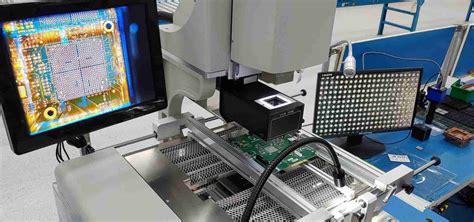
BGA Assembly Equipment
Specialized equipment is required for successful BGA assembly:
- Stencil Printer: Used to apply solder paste to the PCB pads. The stencil ensures precise solder paste deposition.
- Pick-and-Place Machine: Used to accurately place the BGA component onto the PCB. High-precision placement is crucial for proper alignment of the BGA balls with the PCB pads.
- Reflow Oven: Used to melt the solder paste and form the solder joints between the BGA component and PCB. The reflow oven must have accurate temperature control to ensure proper solder joint formation.
- X-ray Inspection System: Used to inspect the solder joints under the BGA package for defects. X-ray inspection is necessary due to the hidden nature of the solder joints.
- Rework Station: Used to remove and replace defective BGA components. The rework station must have precise temperature control to avoid damaging the PCB or adjacent components.

BGA Assembly Challenges
BGA assembly presents several challenges that must be addressed for successful assembly:
1. Thermal Management
BGA packages have a high thermal mass and require careful control of the reflow profile to ensure proper solder joint formation without damaging the component or PCB. Insufficient heating can result in open connections, while excessive heating can cause component or PCB damage.
2. Placement Accuracy
Precise placement of the BGA component onto the PCB is critical for proper alignment of the BGA balls with the PCB pads. Misalignment can result in open or shorted connections.
3. Warpage
BGA packages and PCBs can warp during the reflow process due to the high temperatures involved. Warpage can result in open or shorted connections and must be minimized through proper PCB design and reflow profile control.
4. Inspection Difficulties
The hidden nature of the solder joints under the BGA package makes inspection challenging. X-ray inspection is necessary to detect defects, but can be time-consuming and costly.
5. Rework Challenges
Reworking a defective BGA component is more difficult than reworking other types of components due to the high number of interconnections and hidden solder joints. Specialized equipment and expertise are required for successful BGA rework.
BGA Assembly Best Practices
To ensure successful BGA assembly, several best practices should be followed:
- PCB Design: The PCB should be designed with BGA assembly in mind. This includes providing adequate pad size and spacing, proper via design, and minimizing PCB warpage.
- Stencil Design: The stencil aperture size and shape should be optimized for the specific BGA package to ensure proper solder paste deposition.
- Solder Paste Selection: The solder paste should be selected based on the BGA package type and reflow profile requirements. The solder paste particle size and flux activity level are important considerations.
- Placement Accuracy: The pick-and-place machine should be calibrated and maintained to ensure high placement accuracy. Vision systems can be used to verify proper component alignment before placement.
- Reflow Profile Optimization: The reflow profile should be optimized for the specific BGA package and PCB combination to ensure proper solder joint formation without causing damage. Thermal profiling can be used to verify the reflow profile.
- Inspection and Testing: Comprehensive inspection and testing should be performed after BGA assembly to detect any defects. This includes X-ray inspection, electrical testing, and functional testing as applicable.
- Rework Procedures: Established rework procedures should be in place to address any defects found during inspection and testing. Technicians should be trained in BGA rework techniques.
BGA Assembly Quality Control
Quality control is essential for ensuring reliable BGA assemblies. Key aspects of BGA assembly quality control include:
- Incoming Material Inspection: BGA components and PCBs should be inspected upon receipt to ensure they meet the required specifications. This includes dimensional checks, visual inspection for damage, and electrical testing as applicable.
- Process Control: The BGA assembly process should be monitored and controlled to ensure consistency and quality. This includes regular calibration and maintenance of equipment, monitoring of solder paste deposition and component placement, and verification of reflow profiles.
- Outgoing Quality Control: Completed BGA assemblies should undergo a final quality control inspection before shipment. This includes visual inspection, X-ray inspection of solder joints, and electrical and functional testing as applicable.
- Traceability: A system should be in place to track BGA components and PCBs throughout the assembly process. This allows for quick identification and containment of any quality issues.
- Continuous Improvement: Quality data should be analyzed to identify opportunities for process improvement. This can include root cause analysis of defects, process capability studies, and implementation of corrective and preventive actions.
BGA Assembly Testing
Testing is a critical part of the BGA assembly process to ensure the reliability and functionality of the assembled device. Common BGA assembly testing methods include:
- In-Circuit Testing (ICT): ICT is used to test the electrical connectivity and functionality of the BGA assembly. It involves using a bed-of-nails fixture to make electrical contact with test points on the PCB and verifying the electrical characteristics of the assembly.
- Flying Probe Testing: Flying probe testing is an alternative to ICT that uses movable probes to make electrical contact with test points on the PCB. It offers greater flexibility than ICT but may be slower.
- Boundary Scan Testing: Boundary scan testing, also known as JTAG testing, is used to test the interconnections between BGA components and the PCB. It involves using a boundary scan-enabled device to control and monitor the I/O pins of the BGA components.
- Functional Testing: Functional testing is used to verify that the assembled device functions as intended. It involves subjecting the device to its intended operating conditions and verifying its performance.
BGA Rework Techniques
When a defect is found in a BGA assembly, rework may be necessary to replace the defective component. BGA rework techniques include:
- Localized Heating: Localized heating involves using a focused heat source, such as a hot air pencil or laser, to melt the solder joints of the BGA component. The defective component is then removed and replaced with a new one.
- Global Heating: Global heating involves using a reflow oven to melt the solder joints of the BGA component. The defective component is then removed and replaced with a new one. Global heating is less precise than localized heating but may be necessary for larger BGA components.
- Reballing: Reballing involves removing the solder balls from a defective BGA component and replacing them with new solder balls. This technique is used when the BGA component itself is not defective but the solder balls are damaged or contaminated.
BGA Assembly Cost Considerations
BGA assembly is generally more expensive than assembly of other types of components due to the specialized equipment and expertise required. Factors that affect BGA assembly cost include:
- Component Cost: BGA components are generally more expensive than other types of components due to their high pin count and dense packaging.
- PCB Design: PCBs designed for BGA assembly may be more expensive than PCBs designed for other types of components due to the tighter tolerances and more complex design rules required.
- Assembly Equipment: The specialized equipment required for BGA assembly, such as pick-and-place machines and X-ray inspection systems, can be expensive to purchase and maintain.
- Labor Cost: BGA assembly requires skilled technicians and engineers, which can increase labor costs compared to assembly of simpler components.
- Testing and Inspection: The extensive testing and inspection required for BGA assemblies can add significant cost, particularly if X-ray inspection is required.
BGA Assembly Service Providers
Many electronics manufacturers outsource BGA assembly to specialized service providers. When selecting a BGA assembly service provider, several factors should be considered:
- Experience: The service provider should have extensive experience in BGA assembly and a track record of success.
- Equipment: The service provider should have state-of-the-art equipment for BGA assembly, including high-precision pick-and-place machines, reflow ovens, and X-ray inspection systems.
- Quality Management: The service provider should have a robust quality management system in place, including documented processes, statistical process control, and continuous improvement initiatives.
- Technical Support: The service provider should offer technical support and expertise to help with PCB design, component selection, and troubleshooting.
- Capacity and Lead Time: The service provider should have sufficient capacity to meet the manufacturer’s volume requirements and be able to deliver assembled PCBs in a timely manner.
Future Trends in BGA Assembly
As electronic devices continue to become smaller and more complex, BGA assembly technology will continue to evolve. Some future trends in BGA assembly include:
- Finer Pitch BGA Packages: The pitch (distance between balls) of BGA packages is expected to continue to decrease, allowing for even higher interconnection densities.
- Advanced Materials: New materials, such as advanced substrates and low-temperature solders, are being developed to improve the reliability and thermal performance of BGA assemblies.
- Automation: Continued advancements in automation technology, such as robotic pick-and-place machines and automated optical inspection systems, will improve the speed, accuracy, and consistency of BGA assembly.
- 3D Packaging: 3D packaging technologies, such as package-on-package (PoP) and through-silicon via (TSV), are being developed to allow for even higher levels of integration and miniaturization.
Conclusion
BGA assembly is a critical technology for the production of high-density, high-performance electronic devices. While BGA assembly presents unique challenges compared to assembly of other types of components, careful process control, specialized equipment, and skilled technicians can ensure reliable, high-quality BGA assemblies. As electronic devices continue to become smaller and more complex, BGA assembly technology will continue to evolve to meet the demands of the industry.
Frequently Asked Questions (FAQ)
- What is BGA assembly?
- BGA (Ball Grid Array) assembly is the process of attaching and soldering BGA components onto a printed circuit board (PCB). BGA packages have a grid of solder balls on the bottom that connect to corresponding pads on the PCB.
- What are the advantages of BGA assembly?
- BGA assembly offers several advantages, including high interconnection density, improved signal integrity, small package size, better thermal performance, and high reliability when properly assembled.
- What equipment is used for BGA assembly?
- BGA assembly requires specialized equipment, including stencil printers for applying solder paste, high-precision pick-and-place machines for component placement, reflow ovens for solder joint formation, X-ray inspection systems for defect detection, and rework stations for component replacement.
- What are the challenges of BGA assembly?
- BGA assembly presents several challenges, such as thermal management during reflow soldering, achieving high placement accuracy, minimizing PCB and component warpage, inspecting hidden solder joints, and performing rework on defective components.
- How can I ensure the quality of BGA assemblies?
- To ensure the quality of BGA assemblies, implement comprehensive quality control measures, including incoming material inspection, process control and monitoring, outgoing quality control, traceability, and continuous improvement initiatives. Additionally, perform thorough testing, such as in-circuit testing, flying probe testing, boundary scan testing, and functional testing, to verify the reliability and functionality of the assembled devices.
| Advantage | Description |
|---|---|
| High Density Interconnections | BGAs allow for a high number of interconnections between the IC and PCB in a small package size. |
| Better Signal Integrity | The short lead lengths in BGA packages result in better electrical performance and signal integrity compared to other package types with longer leads. |
| Small Package Size | BGA packages have a small footprint, allowing for more compact PCB designs and higher component density. |
| Improved Thermal Performance | The ball grid array provides a good thermal path from the IC to the PCB, allowing for better heat dissipation. |
| Reliability | When properly assembled, BGA packages offer high reliability due to the low stress on the solder joints. |
| Equipment | Purpose |
|---|---|
| Stencil Printer | Used to apply solder paste to the PCB pads. The stencil ensures precise solder paste deposition. |
| Pick-and-Place Machine | Used to accurately place the BGA component onto the PCB. High-precision placement is crucial for proper alignment of the BGA balls with the PCB pads. |
| Reflow Oven | Used to melt the solder paste and form the solder joints between the BGA component and PCB. The reflow oven must have accurate temperature control to ensure proper solder joint formation. |
| X-ray Inspection System | Used to inspect the solder joints under the BGA package for defects. X-ray inspection is necessary due to the hidden nature of the solder joints. |
| Rework Station | Used to remove and replace defective BGA components. The rework station must have precise temperature control to avoid damaging the PCB or adjacent components. |
| Testing Method | Description |
|---|---|
| In-Circuit Testing (ICT) | ICT is used to test the electrical connectivity and functionality of the BGA assembly. It involves using a bed-of-nails fixture to make electrical contact with test points on the PCB and verifying the electrical characteristics of the assembly. |
| Flying Probe Testing | Flying probe testing is an alternative to ICT that uses movable probes to make electrical contact with test points on the PCB. It offers greater flexibility than ICT but may be slower. |
| Boundary Scan Testing | Boundary scan testing, also known as JTAG testing, is used to test the interconnections between BGA components and the PCB. It involves using a boundary scan-enabled device to control and monitor the I/O pins of the BGA components. |
| Functional Testing | Functional testing is used to verify that the assembled device functions as intended. It involves subjecting the device to its intended operating conditions and verifying its performance. |
Leave a Reply