Overview of PCB Assembly
PCB assembly is the process of attaching electronic components to a printed circuit board. The primary goal is to create a functional electronic device by establishing electrical connections between the components and the board. The process involves several stages, including component placement, soldering, inspection, and testing.
Types of PCB Assembly
There are two main types of PCB assembly:
-
Through-Hole Assembly (THA): In this method, components with long leads are inserted through holes drilled in the PCB and soldered on the opposite side.
-
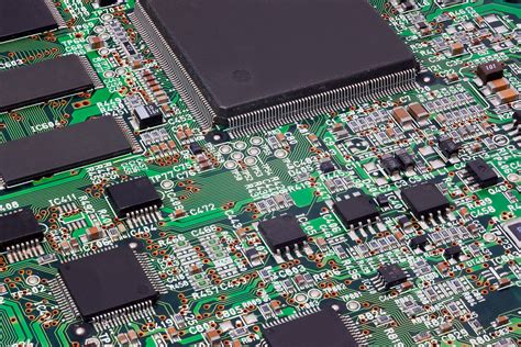
Surface Mount Assembly (SMA): This technique involves placing components directly onto the surface of the PCB and soldering them in place. SMA is more common in modern electronics due to its ability to accommodate smaller components and higher component density.
Steps in the PCB Assembly Process
The PCB assembly process consists of several key steps, each playing a vital role in the creation of a functional electronic device.
1. PCB Design and Fabrication
The first step in the assembly process is the design and fabrication of the printed circuit board itself. This involves creating a schematic diagram, which represents the electrical connections between components, and a layout diagram, which shows the physical placement of components on the board.
Once the design is finalized, the PCB is fabricated using a combination of chemical etching, drilling, and plating processes. The result is a bare PCB ready for component assembly.
2. Solder Paste Application
Before components can be placed on the PCB, a layer of solder paste is applied to the board’s surface. Solder paste is a mixture of tiny solder particles suspended in a flux medium. The paste is typically applied using a Stencil printing process, which ensures precise and consistent application.
3. Component Placement
With the solder paste in place, the next step is to position the electronic components on the PCB. This is done using automated pick-and-place machines, which can rapidly and accurately place components based on the layout diagram.
For through-hole components, the leads are inserted into the corresponding holes in the PCB. Surface mount components are placed directly onto the solder paste on the board’s surface.
4. Reflow Soldering
After component placement, the PCB undergoes a reflow soldering process. The board is passed through a reflow oven, which heats the solder paste to its melting point. As the solder melts, it forms electrical and mechanical connections between the components and the PCB.
The reflow soldering process is carefully controlled to ensure proper solder joint formation and to prevent damage to the components or the board.
5. Inspection and Quality Control
Once the soldering process is complete, the PCB undergoes a series of inspections and quality control checks. These may include:
-
Visual Inspection: A manual or automated visual inspection to identify any visible defects, such as misaligned components, solder bridges, or insufficient solder joints.
-
Automated Optical Inspection (AOI): An automated system that uses cameras and image processing software to detect assembly defects.
-
X-Ray Inspection: Used to examine solder joints and other hidden features that cannot be seen with visual inspection methods.
-
Functional Testing: The PCB is powered on and tested to ensure that it functions as intended and meets the specified performance criteria.
6. Rework and Repair
If any defects are found during the inspection and testing process, the PCB may need to undergo rework or repair. This involves removing and replacing faulty components, repairing damaged solder joints, or making other necessary modifications to bring the board up to the required quality standards.

Technologies Used in PCB Assembly
Modern PCB assembly relies on a range of advanced technologies to ensure efficiency, accuracy, and reliability.
Automated Pick-and-Place Machines
Pick-and-place machines are essential for the rapid and precise placement of components on the PCB. These machines use computer-controlled robotic arms equipped with vacuum nozzles or grippers to pick up components from feeders and place them onto the board.
| Machine Type | Placement Speed (components per hour) | Placement Accuracy |
|---|---|---|
| High-Speed | 50,000 – 100,000+ | ±50 to ±30 microns |
| Mid-Range | 10,000 – 50,000 | ±50 to ±30 microns |
| Entry-Level | Up to 10,000 | ±100 to ±50 microns |
Reflow Soldering Equipment
Reflow soldering is typically performed using convection ovens, which use hot air to melt the solder paste and form solder joints. These ovens are equipped with multiple heating zones and cooling zones to precisely control the temperature profile during the soldering process.
| Oven Type | Heating Method | Temperature Range | Typical Conveyor Speed |
|---|---|---|---|
| Convection | Forced Hot Air | Up to 350°C | 30 – 150 cm/min |
| Vapor Phase | Vapor Condensation | 230 – 260°C | 30 – 120 cm/min |
| Infrared (IR) | Infrared Radiation | Up to 400°C | 30 – 150 cm/min |
Inspection Systems
Various inspection technologies are used to ensure the quality of the assembled PCBs:
- Automated Optical Inspection (AOI): Uses cameras and image processing software to detect surface-level defects.
- Automated X-Ray Inspection (AXI): Employs X-ray imaging to examine solder joints and other hidden features.
- In-Circuit Testing (ICT): Verifies the functionality of individual components and circuits on the PCB using a bed-of-nails fixture.

Best Practices in PCB Assembly
To ensure high-quality and reliable PCB assembly, manufacturers adhere to several best practices:
-
Design for Manufacturing (DFM): Designing PCBs with manufacturing considerations in mind, such as component placement, trace routing, and solder mask application, to improve assembly efficiency and yield.
-
Process Control: Implementing strict process controls, including temperature profiles, solder paste deposition, and component placement accuracy, to maintain consistency and minimize defects.
-
Traceability: Maintaining detailed records of materials, processes, and test results to enable traceability and facilitate root cause analysis in case of issues.
-
Continuous Improvement: Regularly reviewing and optimizing assembly processes based on data analysis, operator feedback, and industry best practices to drive continuous improvement in quality and efficiency.

Frequently Asked Questions (FAQ)
-
What is the difference between through-hole and surface mount assembly?
Through-hole assembly involves inserting component leads through holes in the PCB and soldering them on the opposite side, while surface mount assembly places components directly onto the PCB surface and solders them in place. -
What is solder paste, and how is it applied to the PCB?
Solder paste is a mixture of tiny solder particles suspended in a flux medium. It is typically applied to the PCB using a stencil printing process, which ensures precise and consistent application. -
What is the purpose of reflow soldering in PCB assembly?
Reflow soldering is used to melt the solder paste and form electrical and mechanical connections between the components and the PCB. The process is carefully controlled to ensure proper solder joint formation and prevent damage to the components or the board. -
What types of inspections are performed on assembled PCBs?
Assembled PCBs undergo various inspections, including visual inspection, automated optical inspection (AOI), X-ray inspection, and functional testing, to identify defects and ensure the board meets the required quality standards. -
What are some best practices followed in PCB assembly?
Best practices in PCB assembly include design for manufacturing (DFM), strict process control, maintaining traceability, and continuous improvement based on data analysis and industry best practices.
Conclusion
PCB assembly is a complex and critical process in the production of electronic devices. By understanding the steps involved, the technologies used, and the best practices followed, manufacturers can ensure high-quality and efficient assembly of printed circuit boards. As electronic devices continue to evolve and become more sophisticated, the importance of reliable and precise PCB assembly will only continue to grow.
Leave a Reply