Introduction to Tenting Via in PCB Fabrication
In the world of printed Circuit Board (PCB) fabrication, tenting via is a crucial process that plays a significant role in ensuring the reliability and functionality of the final product. Tenting via refers to the practice of covering the via holes on a PCB with a layer of solder mask, which serves as a protective barrier against environmental factors and potential short circuits.
What is a Via?
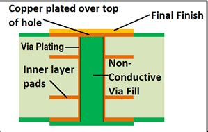
Before diving into the specifics of tenting via, it’s essential to understand what a via is and its purpose in PCB design. A via, short for “vertical interconnect access,” is a small hole drilled through the layers of a PCB to create an electrical connection between different layers. Vias allow signals to travel from one layer to another, enabling more complex routing and efficient use of space on the PCB.
There are several types of vias used in PCB fabrication:
| Via Type | Description |
|---|---|
| Through Hole Via | A via that goes through all layers of the PCB |
| Blind Via | A via that connects an outer layer to an inner layer, but does not go through the entire board |
| Buried Via | A via that connects two or more inner layers, but does not reach the outer layers |
| Micro Via | A small via, typically less than 0.15mm in diameter, used for high-density interconnects |
The Importance of Tenting Via
Tenting via is a critical step in the PCB fabrication process for several reasons:
-
Protection against environmental factors: By covering the via holes with solder mask, tenting via helps protect the exposed copper from oxidation, corrosion, and other environmental factors that could degrade the electrical performance of the PCB over time.
-
Prevention of short circuits: Tenting via prevents solder or other conductive materials from entering the via holes during the soldering process, which could cause short circuits between layers or components.
-
Improved insulation: The solder mask used for tenting via acts as an insulating layer, increasing the overall insulation between the layers of the PCB and reducing the risk of electrical interference.
-
Enhanced mechanical stability: Tenting via helps to reinforce the structural integrity of the PCB by providing additional support around the via holes, reducing the likelihood of cracks or damage during handling and assembly.
Tenting Via Process in PCB Fabrication
The tenting via process typically occurs during the Solder Mask Application stage of PCB fabrication. There are two primary methods for applying solder mask to a PCB: liquid photo imageable (LPI) solder mask and dry film solder mask.
Liquid Photo Imageable (LPI) Solder Mask
LPI solder mask is a liquid photopolymer that is applied to the surface of the PCB using a screen printing or spraying process. The key steps in applying LPI solder mask for tenting via are:
-
Cleaning: The PCB surface is cleaned to remove any contaminants or debris that could affect the adhesion of the solder mask.
-
Application: The LPI solder mask is applied to the PCB surface, covering the entire board, including the via holes.
-
Exposure: The PCB is exposed to UV light through a photomask, which selectively cures the solder mask in the desired areas, including over the via holes for tenting.
-
Developing: The unexposed areas of the solder mask are removed using a developer solution, leaving behind the cured solder mask, including the tented vias.
-
Curing: The PCB undergoes a final curing process to fully harden the solder mask and ensure its durability.
Dry Film Solder Mask
Dry film solder mask is a solid photopolymer film that is laminated onto the surface of the PCB. The process for applying dry film solder mask for tenting via is similar to that of LPI solder mask, with a few key differences:
-
Lamination: The dry film solder mask is laminated onto the PCB surface using heat and pressure.
-
Exposure: The PCB is exposed to UV light through a photomask, selectively curing the solder mask in the desired areas, including over the via holes for tenting.
-
Developing: The unexposed areas of the solder mask are removed using a developer solution, leaving behind the cured solder mask, including the tented vias.
-
Curing: The PCB undergoes a final curing process to fully harden the solder mask and ensure its durability.

Factors Affecting Tenting Via Success
Several factors can impact the success and reliability of tenting via in PCB fabrication:
Via Size and Aspect Ratio
The size and aspect ratio of the via holes can significantly influence the effectiveness of tenting via. Smaller via holes with higher aspect ratios (depth to diameter ratio) can be more challenging to tent successfully, as the solder mask may not adequately fill or cover the entire hole. In general, larger via holes with lower aspect ratios are easier to tent reliably.
Solder Mask Material Properties
The properties of the solder mask material, such as its viscosity, surface tension, and curing characteristics, can affect the ability to tent vias effectively. Solder mask materials with lower viscosity and higher surface tension are more likely to fill and cover via holes uniformly, resulting in better tenting performance.
PCB Surface Finish
The surface finish of the PCB can also impact the success of tenting via. Some surface finishes, such as immersion silver or gold, may require additional processing steps or considerations to ensure adequate solder mask adhesion and coverage over the via holes.
Manufacturing Process Control
Proper control and optimization of the manufacturing process parameters, such as solder mask application, exposure, and curing times and temperatures, are essential for achieving consistent and reliable tenting via results. Inadequate process control can lead to incomplete tenting, solder mask defects, or poor adhesion.

Benefits of Tenting Via in PCB Fabrication
Implementing tenting via in PCB fabrication offers several benefits for both manufacturers and end-users:
-
Improved reliability: By protecting via holes from environmental factors and potential short circuits, tenting via enhances the overall reliability and longevity of the PCB.
-
Reduced manufacturing defects: Tenting via helps to minimize the occurrence of manufacturing defects, such as solder bridging or short circuits, which can lead to improved yield and lower production costs.
-
Enhanced signal integrity: The insulating properties of the solder mask used for tenting via can help to reduce electrical noise and interference, contributing to better signal integrity and overall performance of the PCB.
-
Simplified assembly process: Tented vias can simplify the PCB Assembly process by reducing the need for manual inspection and rework, as the via holes are already protected and insulated.
-
Cost-effective solution: Tenting via is a relatively cost-effective method for improving PCB reliability and performance, as it can be easily integrated into the existing fabrication process without significant additional equipment or material costs.

Challenges and Limitations of Tenting Via
Despite its many benefits, tenting via does have some challenges and limitations that should be considered:
-
Incomplete tenting: In some cases, the solder mask may not completely fill or cover the via holes, leading to incomplete tenting and potential reliability issues. This can be more common with smaller via sizes or higher aspect ratios.
-
Solder mask defects: Improper application or curing of the solder mask can result in defects, such as bubbles, pinholes, or cracks, which can compromise the protective properties of the tented vias.
-
Limited application in high-frequency PCBs: For high-frequency PCBs, tenting via may not be the most suitable option, as the solder mask material can impact the impedance and signal propagation characteristics of the vias. In these cases, alternative methods, such as back-drilling or Via-in-Pad, may be more appropriate.
-
Increased manufacturing complexity: Implementing tenting via in the PCB fabrication process can add some complexity and require additional process control measures to ensure consistent and reliable results.
Conclusion
Tenting via is a critical process in PCB fabrication that offers numerous benefits, including improved reliability, reduced manufacturing defects, enhanced signal integrity, and a simplified assembly process. By covering via holes with a protective layer of solder mask, tenting via helps to ensure the long-term performance and functionality of the PCB.
While there are some challenges and limitations associated with tenting via, such as incomplete tenting or solder mask defects, these can be mitigated through proper process control and optimization. For most PCB applications, tenting via remains a cost-effective and reliable solution for improving PCB reliability and performance.
As PCB technology continues to advance, with increasing complexity and miniaturization, the importance of tenting via in ensuring the quality and reliability of these critical components will only continue to grow.
Frequently Asked Questions (FAQ)
-
Q: What is the main purpose of tenting via in PCB fabrication?
A: The main purpose of tenting via is to protect the via holes from environmental factors, prevent short circuits, and improve the overall reliability and performance of the PCB. -
Q: What are the different types of vias used in PCB fabrication?
A: The different types of vias used in PCB fabrication include through hole vias, blind vias, buried vias, and micro vias. -
Q: What are the two primary methods for applying solder mask for tenting via?
A: The two primary methods for applying solder mask for tenting via are liquid photo imageable (LPI) solder mask and dry film solder mask. -
Q: How does via size and aspect ratio affect the success of tenting via?
A: Smaller via holes with higher aspect ratios can be more challenging to tent successfully, as the solder mask may not adequately fill or cover the entire hole. Larger via holes with lower aspect ratios are generally easier to tent reliably. -
Q: Is tenting via suitable for all PCB applications?
A: While tenting via is suitable for most PCB applications, it may not be the most appropriate option for high-frequency PCBs, as the solder mask material can impact the impedance and signal propagation characteristics of the vias. In these cases, alternative methods, such as back-drilling or via-in-pad, may be more suitable.
Leave a Reply