Introduction to Via-in-Pad Technology
Via-in-Pad (VIP) is a technology used in printed circuit board (PCB) design and manufacturing that allows for the placement of vias directly within the surface mount pads of components. This innovative technique has gained popularity in recent years due to its numerous benefits, including improved signal integrity, reduced board size, and enhanced manufacturing efficiency.
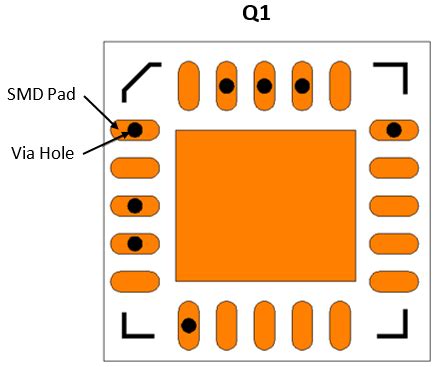
What are Vias?
Before diving into the specifics of Via-in-Pad technology, it’s essential to understand what vias are and their role in PCB design. Vias are small holes drilled through a PCB that allow electrical connections between different layers of the board. They are typically filled with conductive material, such as copper, to create a reliable electrical path.
There are several types of vias commonly used in PCB design:
| Via Type | Description |
|---|---|
| Through Hole Via | Extends through all layers of the PCB |
| Blind Via | Connects an outer layer to an inner layer, but does not go through the entire board |
| Buried Via | Connects inner layers without extending to the outer layers |
| Microvia | A small via with a diameter less than 150 microns, used for high-density interconnects |
Traditional Pad Design vs. Via-in-Pad
In traditional PCB design, vias are placed outside of the component pads, requiring additional space on the board for routing traces. This can lead to larger board sizes and potentially longer signal paths, which may negatively impact signal integrity.
Via-in-Pad technology, on the other hand, allows for the placement of vias directly within the surface mount pads of components. This eliminates the need for additional space around the pads, enabling tighter component placement and more efficient use of board real estate.
Benefits of Via-in-Pad Technology
1. Board Size Reduction
One of the primary advantages of Via-in-Pad technology is its ability to reduce the overall size of a PCB. By placing vias within the component pads, designers can save valuable board space that would otherwise be required for routing traces around the pads. This is particularly beneficial in applications where miniaturization is critical, such as mobile devices, wearables, and IoT devices.
2. Improved Signal Integrity
Via-in-Pad technology can also enhance signal integrity by reducing the length of signal paths. With vias placed directly within the component pads, signals can travel more efficiently from the component to the inner layers of the PCB. This minimizes the potential for signal degradation, crosstalk, and electromagnetic interference (EMI), resulting in better overall performance and reliability.
3. Enhanced Manufacturing Efficiency
Implementing Via-in-Pad technology can streamline the PCB manufacturing process, leading to improved efficiency and cost savings. By eliminating the need for additional routing space around component pads, designers can create more compact and dense layouts. This, in turn, allows for the production of smaller PCBs, which can be manufactured more quickly and with less material waste.

Challenges and Considerations
While Via-in-Pad technology offers numerous benefits, there are also some challenges and considerations to keep in mind when implementing this technique in PCB design and manufacturing.
1. Manufacturing Complexity
Via-in-Pad technology requires precise alignment and drilling of vias within the component pads, which can be more challenging than traditional via placement. Manufacturers must have the necessary equipment and expertise to accurately drill and plate the vias without damaging the pads or compromising the electrical connections.
2. Thermal Management
Placing vias within component pads can impact the thermal performance of the PCB. The vias can act as heat sinks, drawing heat away from the components and into the inner layers of the board. While this can be beneficial in some cases, it may also lead to uneven heat distribution and potential reliability issues if not properly managed.
3. Component Selection
Not all components are suitable for Via-in-Pad design. Some components, particularly those with small or irregularly shaped pads, may not have sufficient space to accommodate vias. Designers must carefully consider the dimensions and layout of the components when deciding whether to implement Via-in-Pad technology.

Via-in-Pad Design Guidelines
To successfully implement Via-in-Pad technology in PCB design, it’s important to follow some key guidelines:
-
Pad Size: Ensure that the component pads are large enough to accommodate the vias without compromising the electrical connections or structural integrity of the pads.
-
Via Size: Choose an appropriate via size based on the component dimensions and the manufacturing capabilities of your PCB fabricator. Smaller vias can enable tighter component placement but may be more challenging to manufacture.
-
Via Placement: Position the vias carefully within the pads to minimize the impact on signal integrity and thermal performance. Avoid placing vias too close to the edges of the pads or in areas that may interfere with the solder joint.
-
Solder Mask Design: Pay close attention to the solder mask design around the Via-in-Pad components. Ensure that there is adequate clearance between the vias and the solder mask openings to prevent solder bridging or other manufacturing defects.
-
DFM Analysis: Conduct a thorough Design for Manufacturability (DFM) analysis to identify any potential issues with your Via-in-Pad design. Work closely with your PCB fabricator to ensure that your design is compatible with their manufacturing processes and capabilities.

Real-World Applications
Via-in-Pad technology has found widespread adoption in various industries and applications where space constraints, signal integrity, and manufacturing efficiency are critical. Some notable examples include:
-
Mobile Devices: Smartphones, tablets, and wearables often require highly compact and dense PCB designs to accommodate the numerous components and features within a limited space. Via-in-Pad technology enables designers to create smaller and more efficient layouts for these devices.
-
IoT Devices: The Internet of Things (IoT) has driven the development of countless connected devices, many of which require miniaturized PCBs to fit within small form factors. Via-in-Pad technology is essential for designing compact and reliable IoT devices.
-
High-Speed Electronics: In applications where signal integrity is paramount, such as high-speed digital circuits and RF devices, Via-in-Pad technology can help minimize signal degradation and ensure optimal performance.
-
Aerospace and Defense: The aerospace and defense industries often require PCBs that can withstand harsh environments and extreme conditions. Via-in-Pad technology can contribute to the development of more robust and reliable electronic systems for these demanding applications.
Frequently Asked Questions (FAQ)
-
Q: Can Via-in-Pad technology be used with any component package type?
A: While Via-in-Pad technology is compatible with many common component package types, such as QFN, BGA, and LGA, some components with small or irregularly shaped pads may not be suitable for this technique. It’s important to carefully consider the dimensions and layout of the components when deciding whether to implement Via-in-Pad technology. -
Q: Does Via-in-Pad technology require special manufacturing processes?
A: Yes, Via-in-Pad technology requires precise alignment and drilling of vias within the component pads, which can be more challenging than traditional via placement. Manufacturers must have the necessary equipment and expertise to accurately drill and plate the vias without damaging the pads or compromising the electrical connections. -
Q: Can Via-in-Pad technology improve the thermal performance of a PCB?
A: In some cases, placing vias within component pads can help dissipate heat more efficiently by acting as heat sinks and drawing heat away from the components and into the inner layers of the board. However, this can also lead to uneven heat distribution if not properly managed, so careful thermal analysis and design are necessary. -
Q: Is Via-in-Pad technology more expensive than traditional PCB design?
A: The cost of implementing Via-in-Pad technology can vary depending on factors such as the complexity of the design, the manufacturing processes required, and the volume of production. While there may be some additional costs associated with the precise alignment and drilling of vias, the overall cost savings from reduced board size and improved manufacturing efficiency can often offset these expenses. -
Q: What are the key benefits of using Via-in-Pad technology in PCB design?
A: The main benefits of Via-in-Pad technology include reduced board size, improved signal integrity, and enhanced manufacturing efficiency. By placing vias directly within component pads, designers can create more compact and dense layouts, minimize signal degradation, and streamline the PCB manufacturing process.
Conclusion
Via-in-Pad technology has revolutionized the way PCBs are designed and manufactured, offering numerous benefits in terms of board size reduction, signal integrity, and manufacturing efficiency. By placing vias directly within the surface mount pads of components, designers can create more compact and reliable electronic systems for a wide range of applications, from mobile devices and IoT to high-speed electronics and aerospace.
However, implementing Via-in-Pad technology also presents some challenges and considerations, such as manufacturing complexity, thermal management, and component selection. To successfully incorporate this technique into PCB design, it’s essential to follow best practices and guidelines, work closely with experienced PCB fabricators, and conduct thorough DFM analysis.
As electronic devices continue to evolve and push the boundaries of miniaturization and performance, Via-in-Pad technology will undoubtedly play an increasingly important role in enabling the development of cutting-edge products across various industries. By understanding the principles, benefits, and challenges of this innovative technique, PCB designers and manufacturers can harness the power of Via-in-Pad technology to create more efficient, reliable, and compact electronic systems for the future.
Leave a Reply