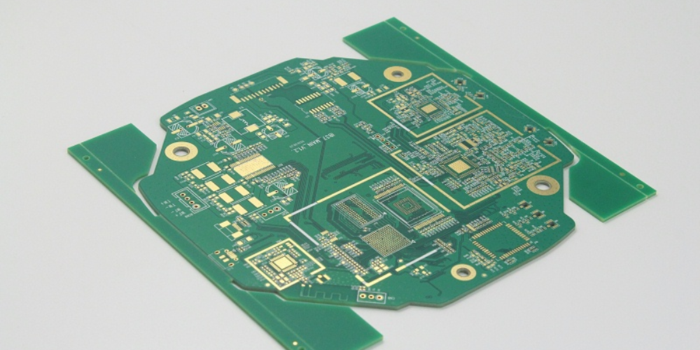
Introduction to Microwave PCBs
Microwave printed circuit boards (PCBs) are circuit boards designed to operate at microwave frequencies, typically above 1 GHz. Unlike traditional PCBs, microwave PCBs require special design considerations to account for effects like dielectric loss, skin effect, and impedance matching at high frequencies.
Microwave PCBs enable various cutting-edge applications in fields like telecommunications, radar, and defense. Their high-frequency capabilities make them integral components of everything from 5G cellular infrastructure to advanced radar systems. As technology continues to advance into higher frequency bands, microwave PCBs will only increase in importance.
Key Design Principles for Microwave PCBs

To function properly at microwave frequencies, microwave PCBs must be designed differently than traditional PCBs. Here are some of the key design principles:
Controlled Impedance
Maintaining a controlled impedance across the PCB is crucial for minimizing signal reflection and power loss at high frequencies. This usually requires careful trace width/spacing control and use of consistent dielectric materials.
| Trace Width | Dielectric Constant | Impedance |
|---|---|---|
| 0.2mm | 4.5 | 50 ohms |
Proper Grounding
At microwave frequencies, currents tend to flow along the surface of conductors. Adequate ground planes on inner layers are needed to provide a return path and prevent radiation. Vias help tie ground layers together.
Minimizing Dielectric Losses
Materials like FR-4 used on regular PCBs have high dielectric losses at microwave frequencies. Low-loss dielectric materials like PTFE or ceramic-filled PTFE are used instead.
Accounting for Skin Effect
Skin effect causes current density to be higher near the surface of traces. Wider, thicker traces help reduce resistive losses.
Impedance Matching
Steps like adding matching circuits help prevent reflections from impedance mismatches. This improves power transfer and frequency response.
Microwave PCB Manufacturing Process
Manufacturing reliable microwave PCBs requires specialized fabrication processes:
- Materials like PTFE and ceramic-filled PTFE are less common than standard FR-4.
- Tight impedance tolerances need to be held across traces. This requires strict process controls.
- PCB panels are often thinner for better heat dissipation at high frequencies. Thin materials can warp and be fragile.
- Smooth copper and precise etching is needed to reduce conductor losses.
- Vias must be properly filled and plated to avoid voids which cause reflections.
Overall, microwave PCB fabrication demands tighter tolerances and performance validation compared to typical PCBs.
Microwave PCB Applications
The unique capabilities of microwave PCBs make them critical enablers for leading-edge systems including:
5G Infrastructure
5G cellular networks operate at mmWave frequencies up to 40 GHz. This requires microwave PCBs in base stations, antennas, and devices.
Satellite Communications
Communications satellites transmit and receive signals from ~3 to 40 GHz. Microwave PCBs help handle these high frequencies.
Radar Systems
Many defense, weather, and aviation radars operate from L-band up to W-band (~1 to 100 GHz). Microwave PCBs are essential RF components.
Scientific Instruments
Test equipment, particle accelerators, radio telescopes, and other scientific gear take advantage of microwaves.
As technology progresses, we can expect microwave PCBs to enable more advanced applications across industries.
Frequently Asked Questions

What are some key differences between microwave PCBs and traditional PCBs?
Microwave PCBs are designed for high frequencies, so they must manage effects like dielectric loss, skin effect, and impedance control. They use special materials and fabrication processes not found in typical PCBs.
Why are low-loss dielectrics important in microwave PCBs?
Low-loss dielectrics like PTFE reduce the dielectric losses that would otherwise greatly attenuate high frequency signals traversing the board.
How does skin effect impact microwave PCB design?
Skin effect causes microwave current to flow mostly near the surface of traces. Wider, thicker traces help mitigate the resistive losses this would otherwise cause.
What applications commonly use microwave PCBs?
Microwave PCBs are critical components in 5G networks, satellite communications, radar systems, scientific instruments, and other advanced microwave and mmWave systems.
How are impedance tolerances controlled in microwave PCB fabrication?
Tight impedance control is achieved through careful process management, including trace dimension tolerances, dielectric thickness and permittivity, and copper surface roughness.
Leave a Reply