What is PCB Silk Screen?
PCB silk screen, also known as legend or nomenclature, is a process used in the manufacturing of printed circuit boards to apply text, logos, and other graphics onto the surface of the board. The silk screen process involves using a fine mesh screen and a stencil to transfer ink onto the PCB surface. This process is an essential part of PCB fabrication as it helps in identifying components, test points, and other important information on the board.
Advantages of PCB Silk Screen
- Improves readability and identification of components
- Enhances the aesthetic appeal of the PCB
- Provides a professional look to the final product
- Helps in the assembly process by guiding the placement of components
- Acts as a reference for debugging and troubleshooting
The Silk Screen Process
Materials Used in PCB Silk Screen
The silk screen process requires the following materials:
- Mesh screen: A fine mesh screen, usually made of polyester or stainless steel, is used to transfer the ink onto the PCB surface.
- Stencil: A stencil with the desired artwork is created and placed on the mesh screen.
- Ink: A special ink, compatible with the PCB surface and resistant to various environmental factors, is used.
- Squeegee: A rubber or plastic blade is used to spread the ink evenly across the stencil and mesh screen.
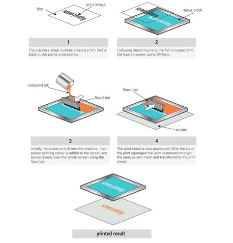
Steps Involved in PCB Silk Screen
- Artwork preparation: The desired artwork, including text and graphics, is created using CAD software.
- Stencil making: A stencil with the artwork is created, usually by photographic methods or laser cutting.
- Screen preparation: The mesh screen is coated with a light-sensitive emulsion and exposed to light with the stencil placed on top. The unexposed areas are then washed away, leaving the artwork on the screen.
- Ink application: The PCB is placed under the screen, and ink is applied using a squeegee. The ink passes through the open areas of the screen, transferring the artwork onto the PCB surface.
- Curing: The printed PCB is then dried and cured, either by air drying or through the use of UV light or heat, to ensure the ink adheres properly to the surface.

Designing for PCB Silk Screen
When designing artwork for PCB silk screen, several factors should be considered to ensure the best results:
- Font size and style: Choose a font that is easily readable and has a minimum size of 0.8mm to ensure clarity.
- Line width: The minimum line width for PCB silk screen should be 0.15mm to ensure proper ink transfer and adhesion.
- Spacing: Maintain adequate spacing between elements to prevent ink bleeding and maintain readability.
- Color: Most PCB silk screens use white ink, but other colors like black, yellow, or red can be used for specific applications.
- Placement: Position the artwork in a way that does not interfere with component placement or soldering.
| Element | Minimum Size |
|---|---|
| Font Size | 0.8mm |
| Line Width | 0.15mm |

Common Applications of PCB Silk Screen
PCB silk screen is used in various applications across different industries:
- Consumer electronics: Silk screen is used to label components, connectors, and test points on PCBs found in smartphones, laptops, and other electronic devices.
- Industrial equipment: In industrial settings, PCB silk screen is used to label boards in control systems, sensors, and automation equipment.
- Medical devices: Silk screen is crucial in medical device PCBs to ensure proper identification and assembly of components in life-critical systems.
- Automotive electronics: PCBs in vehicles, such as those found in engine control units and infotainment systems, rely on silk screen for labeling and identification.
- Aerospace and defense: High-reliability PCBs used in aerospace and defense applications use silk screen to label components and provide clear instructions for assembly and maintenance.

Challenges and Limitations of PCB Silk Screen
While PCB silk screen is a widely used and essential process, it does have some challenges and limitations:
- Limited resolution: The resolution of silk screen is lower compared to other methods like direct legend printing, which can limit the level of detail in the artwork.
- Ink compatibility: The ink used in silk screen must be compatible with the PCB surface material and the various environmental factors the board will be exposed to, such as temperature and humidity.
- Alignment issues: Misalignment of the screen during the printing process can lead to inaccurate or blurred artwork on the PCB surface.
- Wear and tear: Over time, the silk screen artwork may fade or wear off due to handling or exposure to environmental factors.
Alternative Methods to PCB Silk Screen
While silk screen is the most common method for applying artwork to PCBs, there are alternative methods available:
- Direct legend printing: This process uses a specialized inkjet printer to directly print the artwork onto the PCB surface, offering higher resolution and faster turnaround times.
- Laser etching: A laser is used to etch the artwork directly onto the PCB surface, providing a permanent and high-resolution solution.
- Pad printing: This process uses a silicone pad to transfer ink from a cliché onto the PCB surface, allowing for printing on irregular surfaces.
| Method | Advantages | Disadvantages |
|---|---|---|
| Direct Legend Printing | Higher resolution, faster turnaround | Higher cost, limited color options |
| Laser Etching | Permanent, high resolution | Higher cost, limited color options |
| Pad Printing | Can print on irregular surfaces | Limited resolution, slower process |
The Future of PCB Silk Screen
As PCB technology continues to advance, the silk screen process is also evolving to meet new challenges and requirements:
- Finer resolution: Advances in screen materials and printing techniques are enabling finer resolution artwork, allowing for more detailed and compact designs.
- Improved ink formulations: New ink formulations are being developed to provide better adhesion, durability, and compatibility with a wider range of PCB surface materials.
- Automation: Automated silk screen systems are becoming more prevalent, offering faster throughput, improved consistency, and reduced human error.
- Integration with other processes: Silk screen is being integrated with other PCB fabrication processes, such as solder mask application and surface finishes, to streamline production and improve overall quality.
Frequently Asked Questions (FAQ)
-
Q: What is the minimum font size for PCB silk screen?
A: The minimum recommended font size for PCB silk screen is 0.8mm to ensure readability. -
Q: Can PCB silk screen be used on flexible PCBs?
A: Yes, silk screen can be used on flexible PCBs, but the ink and curing process must be compatible with the flexible substrate material. -
Q: How does PCB silk screen affect the assembly process?
A: PCB silk screen provides clear labels and instructions for component placement, helping to guide the assembly process and reduce errors. -
Q: What is the most common color used for PCB silk screen?
A: White is the most common color used for PCB silk screen, but other colors like black, yellow, or red can be used for specific applications. -
Q: How long does the PCB silk screen process take?
A: The silk screen process typically takes a few hours to complete, depending on the complexity of the artwork and the number of boards being printed. However, the entire PCB fabrication process, including silk screen, can take several days to weeks, depending on the specific requirements of the project.
In conclusion, PCB silk screen is a vital process in the fabrication of printed circuit boards, providing clear labeling, identification, and instructions for assembly and troubleshooting. By understanding the materials, processes, and design considerations involved in PCB silk screen, engineers and manufacturers can ensure the highest quality and reliability in their electronic products. As PCB technology continues to evolve, the silk screen process will also adapt to meet new challenges and requirements, remaining an essential tool in the electronics industry.
Leave a Reply