Introduction to Vias in PCB Design
Vias are an essential component of printed circuit board (PCB) design, allowing electrical connections between different layers of a multi-layer PCB. They are small holes drilled through the PCB and plated with a conductive material, typically copper, to create an electrical pathway. Vias come in various types, each with its own unique characteristics and applications. In this article, we will explore three specific types of vias: tenting vias, plugged vias, and via-in-pad.
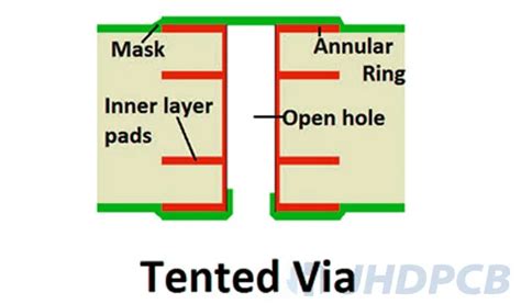
What are Tenting Vias?
Tenting vias, also known as covered vias or mask-defined vias, are vias that are covered with solder mask on one or both sides of the PCB. The solder mask acts as a protective layer, preventing solder from entering the via during the soldering process. Tenting vias are commonly used in high-density PCB designs where space is limited, and it is necessary to place components or traces close to the vias.
Advantages of Tenting Vias
- Improved solder joint reliability: By preventing solder from entering the via, tenting ensures a stronger and more reliable solder joint between the component and the pad.
- Increased component density: Tenting allows components to be placed closer to vias, enabling higher component density on the PCB.
- Enhanced electrical insulation: The solder mask covering the via provides an additional layer of electrical insulation, reducing the risk of short circuits.
- Improved manufacturability: Tenting vias simplifies the soldering process by eliminating the need for special techniques to prevent solder from entering the via.
Disadvantages of Tenting Vias
- Limited thermal dissipation: The solder mask covering the via can impede heat transfer, potentially leading to increased thermal stress on the PCB and components.
- Reduced visual inspection: Tenting vias can make visual inspection of the solder joints more difficult, as the solder mask obscures the view of the via.
What are Plugged Vias?
Plugged vias, also known as filled vias, are vias that are completely filled with a non-conductive material, such as epoxy or resin. The filling material is typically applied using a screen printing process, and then cured to create a solid, non-conductive plug within the via. Plugged vias are used in applications where it is necessary to prevent any electrical connection through the via, such as in high-voltage or high-frequency circuits.
Advantages of Plugged Vias
- Complete electrical isolation: Plugged vias provide complete electrical isolation between the layers of the PCB, eliminating any potential for signal leakage or interference.
- Improved mechanical strength: The solid filling material adds mechanical strength to the via, reducing the risk of via breakage or delamination.
- Enhanced thermal conductivity: Certain filling materials, such as thermally conductive epoxies, can improve the thermal conductivity of the via, helping to dissipate heat more effectively.
Disadvantages of Plugged Vias
- Increased manufacturing complexity: Plugging vias adds an additional step to the PCB manufacturing process, which can increase production time and cost.
- Limited rework ability: Once a via is plugged, it is difficult to rework or repair, as the filling material must be removed before any changes can be made.
- Potential for void formation: If the filling material is not applied properly, voids can form within the via, reducing its mechanical and thermal properties.
What is Via-in-Pad?
Via-in-pad, also known as via-in-pad plating or VIPPs, is a PCB design technique where a via is placed directly within a component pad. This allows for a more compact PCB layout, as the via and pad occupy the same space on the board. Via-in-pad is commonly used in high-density PCB designs, such as those found in smartphones, tablets, and other portable electronic devices.
Advantages of Via-in-Pad
- Increased component density: By placing the via within the pad, via-in-pad allows for a more compact PCB layout, enabling higher component density.
- Improved signal integrity: Via-in-pad minimizes the distance between the component and the via, reducing the risk of signal degradation or interference.
- Enhanced thermal management: Via-in-pad can provide a direct thermal path from the component to the inner layers of the PCB, improving heat dissipation.
- Reduced manufacturing costs: Via-in-pad eliminates the need for additional pads or traces, potentially reducing PCB manufacturing costs.
Disadvantages of Via-in-Pad
- Increased manufacturing complexity: Via-in-pad requires precise alignment between the via and the pad, which can be challenging to achieve consistently in high-volume production.
- Limited pad size: The size of the pad must be large enough to accommodate both the component and the via, which can limit the minimum component size that can be used.
- Potential for solder wicking: If the via is not properly filled or covered, solder can wick into the via during the soldering process, potentially causing a weak or unreliable solder joint.
PCB Design Considerations for Tenting Vias, Plugged Vias, and Via-in-Pad
When incorporating tenting vias, plugged vias, or via-in-pad into a PCB design, there are several key considerations that must be taken into account to ensure optimal performance and manufacturability.
Design Guidelines for Tenting Vias
- Via size: The size of the via should be carefully chosen to ensure adequate electrical and thermal conductivity while minimizing the overall footprint. A smaller via size allows for higher component density but may increase manufacturing complexity.
- Solder mask coverage: The solder mask should completely cover the via on both sides of the PCB to prevent solder from entering the via during the soldering process. The solder mask opening should be slightly larger than the via diameter to account for any misalignment during manufacturing.
- Pad size: The pad surrounding the via should be large enough to accommodate the solder mask opening and provide sufficient space for a reliable solder joint. The pad size should be calculated based on the via size, solder mask coverage, and the specific requirements of the component being used.
- Via placement: Tenting vias should be placed as close to the component as possible to minimize the distance between the component and the via. However, adequate spacing must be maintained between vias and other components or traces to prevent signal interference or short circuits.
Design Guidelines for Plugged Vias
- Via size: The size of the via should be chosen based on the specific electrical and mechanical requirements of the application. Larger vias may be necessary for high-current or high-voltage applications, while smaller vias may be used for signal routing.
- Filling material selection: The filling material should be selected based on the specific requirements of the application, such as electrical insulation, thermal conductivity, and mechanical strength. Common filling materials include epoxy, resin, and conductive inks.
- Filling process: The filling process should be carefully controlled to ensure complete and consistent filling of the via. Incomplete filling can result in voids or air pockets, which can reduce the mechanical and thermal properties of the via.
- Via placement: Plugged vias should be placed in areas of the PCB where electrical isolation is critical, such as between power and ground planes or in high-voltage circuits. Adequate spacing must be maintained between plugged vias and other components or traces to prevent signal interference or short circuits.
Design Guidelines for Via-in-Pad
- Via size: The size of the via should be carefully chosen to ensure adequate electrical and thermal conductivity while minimizing the overall footprint. A smaller via size allows for higher component density but may increase manufacturing complexity.
- Pad size: The pad size must be large enough to accommodate both the component and the via, with sufficient space for a reliable solder joint. The pad size should be calculated based on the specific requirements of the component being used and the size of the via.
- Via placement: The via should be placed as close to the center of the pad as possible to ensure optimal electrical and thermal performance. However, adequate spacing must be maintained between the via and the edge of the pad to prevent solder wicking or other manufacturing defects.
- Solder mask design: The solder mask opening should be designed to expose the entire pad and via, allowing for proper solder joint formation during the soldering process. The solder mask should also be designed to prevent solder from wicking into the via, which can be achieved through the use of plugged or filled vias.

Manufacturing Considerations for Tenting Vias, Plugged Vias, and Via-in-Pad
In addition to PCB design considerations, there are several manufacturing considerations that must be taken into account when incorporating tenting vias, plugged vias, or via-in-pad into a PCB.
Manufacturing Considerations for Tenting Vias
- Solder mask application: The solder mask must be applied consistently and accurately to ensure complete coverage of the via on both sides of the PCB. Inconsistent or incomplete solder mask coverage can result in solder entering the via during the soldering process, potentially causing defects or reliability issues.
- Alignment accuracy: Proper alignment between the via and the solder mask opening is critical to ensure a reliable solder joint. Misalignment can result in exposed copper or solder bridging, which can cause short circuits or other defects.
- Via plating: The via must be properly plated with a conductive material, typically copper, to ensure adequate electrical conductivity. Incomplete or inconsistent plating can result in high resistance or open circuits, which can affect the performance and reliability of the PCB.
Manufacturing Considerations for Plugged Vias
- Filling process control: The filling process must be carefully controlled to ensure complete and consistent filling of the via. Incomplete filling can result in voids or air pockets, which can reduce the mechanical and thermal properties of the via. Overfilling can result in excess material on the surface of the PCB, which can interfere with component placement or soldering.
- Curing process: The filling material must be properly cured to ensure optimal mechanical and thermal properties. Incomplete or inconsistent curing can result in weak or brittle vias, which can affect the reliability and durability of the PCB.
- Material compatibility: The filling material must be compatible with the PCB substrate and other materials used in the manufacturing process, such as solder mask and soldermaterials. Incompatible materials can result in delamination, cracking, or other defects that can affect the performance and reliability of the PCB.
Manufacturing Considerations for Via-in-Pad
- Via filling: The via must be properly filled or plugged to prevent solder from wicking into the via during the soldering process. Incomplete or inconsistent filling can result in weak or unreliable solder joints, which can affect the performance and reliability of the PCB.
- Pad and via alignment: Proper alignment between the pad and the via is critical to ensure a reliable solder joint. Misalignment can result in exposed copper or solder bridging, which can cause short circuits or other defects.
- Soldering process: The soldering process must be carefully controlled to ensure proper solder joint formation without causing solder wicking or other defects. The solder paste volume, stencil design, and reflow profile must be optimized for the specific component and via-in-pad design being used.

Testing and Inspection Techniques for Tenting Vias, Plugged Vias, and Via-in-Pad
To ensure the quality and reliability of PCBs incorporating tenting vias, plugged vias, or via-in-pad, several testing and inspection techniques can be employed during the manufacturing process.
Testing and Inspection Techniques for Tenting Vias
- Visual inspection: Visual inspection can be used to verify the proper placement and coverage of the solder mask over the vias. Any defects or inconsistencies in the solder mask coverage can be identified and corrected before the soldering process.
- Automated optical inspection (AOI): AOI can be used to automatically inspect the solder mask coverage and alignment over the vias. AOI systems can quickly identify any defects or inconsistencies in the solder mask coverage, allowing for early detection and correction of issues.
- Electrical testing: Electrical testing can be used to verify the electrical conductivity and isolation of the vias. Resistance testing can be used to ensure that the vias are properly plated and have low resistance, while insulation resistance testing can be used to ensure that the solder mask provides adequate electrical isolation.
Testing and Inspection Techniques for Plugged Vias
- Visual inspection: Visual inspection can be used to verify the complete and consistent filling of the vias. Any voids, air pockets, or inconsistencies in the filling can be identified and corrected before the curing process.
- X-ray inspection: X-ray inspection can be used to non-destructively inspect the internal structure of the plugged vias. X-ray imaging can reveal any voids, cracks, or other defects within the filling material that may not be visible from the surface.
- Cross-sectional analysis: Cross-sectional analysis can be used to destructively inspect the internal structure of the plugged vias. By cutting the PCB and examining the cross-section of the via, the complete and consistent filling of the via can be verified, and any defects or inconsistencies can be identified.
Testing and Inspection Techniques for Via-in-Pad
- Visual inspection: Visual inspection can be used to verify the proper placement and alignment of the via within the pad. Any misalignment or exposed copper can be identified and corrected before the soldering process.
- X-ray inspection: X-ray inspection can be used to non-destructively inspect the internal structure of the via and the solder joint. X-ray imaging can reveal any voids, cracks, or other defects within the via or the solder joint that may not be visible from the surface.
- Microsectioning: Microsectioning can be used to destructively inspect the internal structure of the via and the solder joint. By cutting the PCB and examining the cross-section of the via and the solder joint, the complete and consistent filling of the via and the quality of the solder joint can be verified, and any defects or inconsistencies can be identified.

Common Defects and Failure Modes for Tenting Vias, Plugged Vias, and Via-in-Pad
Despite careful design and manufacturing considerations, defects and failures can still occur in PCBs incorporating tenting vias, plugged vias, or via-in-pad. Understanding the common defects and failure modes associated with each via type can help in identifying and correcting issues early in the manufacturing process.
Common Defects and Failure Modes for Tenting Vias
- Solder mask coverage defects: Inconsistent or incomplete solder mask coverage over the vias can result in solder entering the via during the soldering process, potentially causing short circuits or other defects. Solder mask coverage defects can be caused by improper solder mask application, misalignment, or damage during handling.
- Via plating defects: Incomplete or inconsistent via plating can result in high resistance or open circuits, which can affect the performance and reliability of the PCB. Via plating defects can be caused by improper plating processes, contamination, or damage during handling.
- Solder joint defects: Weak or unreliable solder joints can occur if solder enters the via during the soldering process, or if the solder mask coverage is inadequate. Solder joint defects can be caused by improper solder paste volume, incorrect reflow profiles, or contamination.
Common Defects and Failure Modes for Plugged Vias
- Filling defects: Incomplete or inconsistent filling of the vias can result in voids, air pockets, or other defects that can reduce the mechanical and thermal properties of the via. Filling defects can be caused by improper filling processes, incorrect material viscosity, or contamination.
- Curing defects: Incomplete or inconsistent curing of the filling material can result in weak or brittle vias, which can affect the reliability and durability of the PCB. Curing defects can be caused by incorrect curing temperatures, times, or environments.
- Material compatibility issues: Incompatible filling materials can result in delamination, cracking, or other defects that can affect the performance and reliability of the PCB. Material compatibility issues can be caused by incorrect material selection, improper curing, or contamination.
Common Defects and Failure Modes for Via-in-Pad
- Via filling defects: Incomplete or inconsistent filling of the via can result in solder wicking into the via during the soldering process, potentially causing weak or unreliable solder joints. Via filling defects can be caused by improper filling processes, incorrect material viscosity, or contamination.
- Pad and via misalignment: Misalignment between the pad and the via can result in exposed copper or solder bridging, which can cause short circuits or other defects. Pad and via misalignment can be caused by incorrect PCB design, manufacturing tolerances, or handling.
- Solder joint defects: Weak or unreliable solder joints can occur if solder wicks into the via, or if the solder paste volume or reflow profile is incorrect. Solder joint defects can be caused by improper via filling, incorrect solder paste volume, incorrect reflow profiles, or contamination.
Frequently Asked Questions (FAQ)
- What is the difference
Leave a Reply