Introduction to RAYPCB and Multi-layer PCBs
RAYPCB, a leading printed circuit board (PCB) manufacturer, has recently announced an update to its standard stackup for multi-layer PCBs. This update aims to enhance the performance, reliability, and manufacturing efficiency of their PCB products. In this article, we will explore the significance of this update and how it benefits customers in various industries.
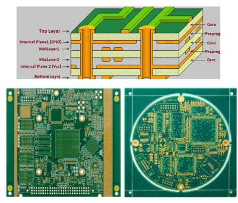
What is a Multi-layer PCB?
A multi-layer PCB is a printed circuit board that consists of three or more conductive copper layers laminated together with insulating material. These layers are interconnected through vias, which are small holes drilled through the board and plated with conductive material. Multi-layer PCBs offer several advantages over single or double-layer boards, including:
- Increased circuit density and complexity
- Improved signal integrity and reduced electromagnetic interference (EMI)
- Better heat dissipation and mechanical stability
- Reduced overall board size and weight
RAYPCB’s Commitment to Quality and Innovation
RAYPCB has been providing high-quality PCB solutions for over a decade, catering to customers in various sectors such as telecommunications, automotive, industrial, and consumer electronics. The company’s success can be attributed to its commitment to continuous improvement, advanced manufacturing capabilities, and customer-centric approach.
By updating its standard stackup for multi-layer PCBs, RAYPCB demonstrates its dedication to staying at the forefront of PCB technology and meeting the evolving needs of its customers.
Key Features of RAYPCB’s Updated Standard Stackup
Optimized Layer Configuration
One of the primary aspects of RAYPCB’s updated standard stackup is the optimized layer configuration. The new stackup incorporates a strategic arrangement of signal, power, and ground layers to maximize signal integrity and minimize noise and crosstalk.
| Layer | Function |
|---|---|
| Top | Signal |
| L2 | Ground |
| L3 | Signal |
| L4 | Power |
| L5 | Signal |
| L6 | Ground |
| Bottom | Signal |
This configuration ensures that critical signals are shielded by adjacent ground planes, reducing electromagnetic interference and improving overall signal quality. The power layer is strategically placed near the center of the stackup to provide a stable and low-impedance power distribution network.
Enhanced Material Selection
RAYPCB has carefully selected the materials used in its updated standard stackup to optimize performance and reliability. The company now uses high-quality, low-loss dielectric materials that offer excellent electrical properties and thermal stability.
| Material | Dielectric Constant | Dissipation Factor | Thermal Conductivity (W/mK) |
|---|---|---|---|
| FR-4 | 4.5 | 0.02 | 0.3 |
| Isola 370HR | 3.7 | 0.01 | 0.4 |
| Rogers 4350B | 3.5 | 0.0037 | 0.6 |
By using these advanced materials, RAYPCB can deliver PCBs with lower dielectric losses, improved thermal management, and better overall performance, especially at higher frequencies.
Improved Impedance Control
Impedance control is crucial for maintaining signal integrity and ensuring proper functioning of high-speed circuits. RAYPCB’s updated standard stackup incorporates stricter impedance control measures to meet the demanding requirements of modern electronic devices.
The company now offers tighter tolerances on controlled impedance traces, with a typical tolerance of ±10% for single-ended traces and ±5% for differential pairs. This level of precision is achieved through advanced manufacturing processes, such as fine-line etching and controlled dielectric thickness.
Enhanced Via Technology
Vias play a critical role in multi-layer PCBs, providing interconnections between layers. RAYPCB has implemented advanced via technologies in its updated standard stackup to minimize signal degradation and improve reliability.
-
Microvias: Microvias are small, laser-drilled vias that offer higher density and improved signal integrity compared to traditional mechanically drilled vias. RAYPCB now employs microvia technology in its standard stackup, enabling customers to design more complex and compact PCBs.
-
Filled and Capped Vias: To enhance the mechanical strength and thermal conductivity of the PCB, RAYPCB offers filled and capped vias as part of its standard stackup. Filled vias are plugged with a conductive material, while capped vias have an additional copper layer applied over the top and bottom surfaces. These techniques help to reduce thermal stress and improve the overall reliability of the PCB.

Benefits of RAYPCB’s Updated Standard Stackup
Improved Signal Integrity and Performance
By optimizing the layer configuration, material selection, impedance control, and via technology, RAYPCB’s updated standard stackup significantly improves signal integrity and overall PCB performance. Customers can expect their designs to have:
- Reduced signal loss and distortion
- Minimized crosstalk and electromagnetic interference
- Improved signal-to-noise ratio
- Better power integrity and thermal management
These enhancements enable customers to develop more advanced and reliable electronic products, meeting the ever-increasing demands of their respective industries.
Faster Time-to-Market and Cost Savings
RAYPCB’s updated standard stackup not only improves PCB performance but also streamlines the manufacturing process. By standardizing the layer configuration and material selection, the company can reduce lead times and minimize the risk of manufacturing errors.
Moreover, the improved via technology and impedance control measures incorporated in the standard stackup help to reduce the need for multiple design iterations and prototype runs. This translates to faster time-to-market for customers, as well as potential cost savings associated with reduced design and manufacturing cycles.
Versatility and Scalability
The updated standard stackup is designed to cater to a wide range of applications and industries. Whether customers require high-speed digital circuits, analog sensors, or power electronics, RAYPCB’s new stackup can be easily adapted to meet their specific needs.
Furthermore, the standard stackup is scalable, allowing customers to easily transition from prototype to high-volume production without significant changes to the PCB design or manufacturing process. This scalability ensures a smooth and cost-effective production ramp-up, enabling customers to bring their products to market quickly and efficiently.

Real-World Applications and Success Stories
Telecommunications Industry
One of RAYPCB’s customers in the telecommunications industry required a high-speed, low-loss PCB for their latest 5G base station equipment. By leveraging the updated standard stackup, RAYPCB was able to deliver a PCB that met the customer’s stringent performance requirements while reducing the overall design and manufacturing time by 20%.
The optimized layer configuration and enhanced material selection of the new stackup enabled the customer to achieve superior signal integrity and thermal management, resulting in a more reliable and efficient 5G base station.
Automotive Industry
An automotive electronics manufacturer approached RAYPCB with a challenge to develop a compact, high-density PCB for their advanced driver assistance system (ADAS). Using the updated standard stackup, RAYPCB successfully designed and manufactured a PCB that incorporated fine-pitch components and high-speed interfaces while maintaining excellent signal integrity and reliability.
The improved via technology and impedance control measures of the new stackup allowed the customer to minimize signal distortion and crosstalk, ensuring the proper functioning of the ADAS even in harsh automotive environments.
Industrial Automation
A leading industrial automation company required a robust and reliable PCB for their motor control system. RAYPCB’s updated standard stackup provided the perfect solution, offering enhanced thermal management and mechanical stability.
The optimized power layer configuration and the use of high-quality, low-loss materials in the new stackup helped to reduce power dissipation and improve the overall efficiency of the motor control system. The customer reported a 15% increase in system reliability and a 10% reduction in energy consumption.

Frequently Asked Questions (FAQ)
-
Q: What is the minimum layer count supported by RAYPCB’s updated standard stackup?
A: RAYPCB’s updated standard stackup supports a minimum of 4 layers, with options for 6, 8, 10, and 12 layers available. -
Q: Can I request customizations to the standard stackup for my specific application?
A: Yes, RAYPCB offers customization options for customers with specific requirements. Our experienced engineering team will work closely with you to develop a tailored stackup that meets your needs. -
Q: What is the maximum operating frequency supported by the updated standard stackup?
A: The maximum operating frequency depends on various factors such as the dielectric material, layer configuration, and trace geometry. RAYPCB’s updated standard stackup can support frequencies up to 20 GHz for high-speed applications, with proper design considerations. -
Q: Are there any limitations on the PCB Size or aspect ratio when using the updated standard stackup?
A: RAYPCB’s standard stackup can accommodate a wide range of PCB sizes and aspect ratios. However, for very large or highly asymmetrical designs, additional considerations may be necessary to ensure manufacturability and reliability. -
Q: How does the updated standard stackup compare to RAYPCB’s previous stackup in terms of cost?
A: While the updated standard stackup incorporates advanced materials and technologies, RAYPCB has optimized its manufacturing processes to minimize any cost impact. In many cases, the improved performance and reliability offered by the new stackup can lead to long-term cost savings for customers.
Conclusion
RAYPCB’s updated standard stackup for multi-layer PCBs represents a significant advancement in PCB technology, offering improved performance, reliability, and manufacturing efficiency. By optimizing the layer configuration, material selection, impedance control, and via technology, RAYPCB is enabling customers across various industries to develop more advanced and reliable electronic products.
The benefits of the updated standard stackup, including improved signal integrity, faster time-to-market, cost savings, versatility, and scalability, make it an attractive choice for customers seeking high-quality PCB solutions. As demonstrated by the success stories from the telecommunications, automotive, and industrial automation sectors, RAYPCB’s new stackup is already proving its value in real-world applications.
As the electronics industry continues to evolve and demand more from PCB manufacturers, RAYPCB remains committed to staying at the forefront of technology and providing its customers with the best possible solutions. The updated standard stackup is just one example of how the company is continuously innovating to meet the needs of its customers and drive the future of the PCB industry.
Leave a Reply