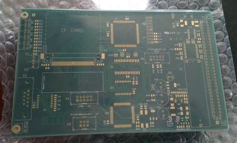
What is ENIG?
Electroless Nickel Immersion Gold (ENIG) is a popular surface finish for printed circuit boards (PCBs). It provides excellent solderability, flatness, and corrosion resistance for PCB pads and through-holes. ENIG consists of an electroless nickel plating layer covered by a thin immersion gold layer.
ENIG offers several advantages over other surface finishes like HASL (Hot Air Solder Leveling), OSP (Organic Solderability Preservatives), and Immersion Silver:
- Flat surface ideal for fine-pitch components
- Excellent solderability and wettability
- Corrosion and oxidation resistant finish
- Resistant to multiple reflow cycles
- Good electrical conductivity
- Harder, more wear-resistant surface
- Suitable for gold wire bonding
- RoHS compliant lead-free finish
ENIG Layer Composition
The ENIG surface finish consists of two primary layers:
- Electroless Nickel (Ni) Layer:
- Typical thickness: 3-6 μm
- Acts as a barrier layer to prevent copper diffusion
- Provides a smooth, uniform surface for gold deposition
-
Increases durability and wear resistance
-
Immersion Gold (Au) Layer:
- Typical thickness: 0.05-0.2 μm (1.97-7.87 μin)
- Protects the nickel layer from oxidation
- Enhances solderability and wettability
- Facilitates gold wire bonding
- Gives the surface a gold appearance
The ENIG Process at RAYPCB
At RAYPCB, we follow a well-established process to produce high-quality ENIG PCBs. The process involves several steps:
-
Cleaning: The PCB surface is thoroughly cleaned to remove any contaminants or oxides.
-
Microetching: A mild etching solution is used to roughen the copper surface for better adhesion of the nickel layer.
-
Catalyzation: The PCB is immersed in a catalytic solution containing palladium, which acts as a catalyst for the electroless nickel deposition.
-
Electroless Nickel Plating: The PCB is placed in an electroless nickel bath, where the nickel layer is uniformly deposited on the copper surface through an autocatalytic chemical reaction.
-
Immersion Gold Plating: The nickel-plated PCB is then immersed in a gold bath, where a thin layer of gold is deposited on the nickel surface through a displacement reaction.
-
Rinsing and Drying: The ENIG-plated PCB is rinsed with deionized water and dried using hot air or nitrogen.
-
Inspection: The finished ENIG PCB undergoes a thorough visual and electrical inspection to ensure quality and conformance to specifications.

ENIG Specifications at RAYPCB
At RAYPCB, we adhere to the following specifications for our ENIG surface finish:
| Parameter | Specification |
|---|---|
| Nickel Thickness | 3-6 μm |
| Gold Thickness | 0.05-0.2 μm (1.97-7.87 μin) |
| Surface Roughness (Ra) | ≤ 0.5 μm |
| Solderability | PASS, IPC-J-STD-003 |
| Solder Wettability | > 95% coverage |
| Salt Spray Test | > 120 hours, ASTM B117 |

Designing for ENIG
When designing PCBs for ENIG surface finish, consider the following guidelines:
-
Pad and Via Sizes: Ensure that pad and via sizes are appropriate for the ENIG process. Minimum recommended pad size is 0.2 mm (7.87 mil) and minimum via size is 0.3 mm (11.81 mil).
-
Solder Mask Design: Use a solder mask to protect the ENIG surface from oxidation and contamination. Ensure that the solder mask apertures are slightly larger than the pad size to accommodate the ENIG plating.
-
Copper Surface Preparation: The copper surface should be clean and free of contaminants before the ENIG process. Ensure that the PCB design allows for proper cleaning and microetching.
-
Thermal Considerations: ENIG has a lower thermal conductivity compared to bare copper. Consider this when designing for high-power or heat-sensitive applications.
-
Gold Wire Bonding: If gold wire bonding is required, specify the gold thickness accordingly. A minimum gold thickness of 0.075 μm (2.95 μin) is recommended for wire bonding.

Advantages of Choosing RAYPCB for ENIG
At RAYPCB, we offer high-quality ENIG surface finish for your PCBs with several advantages:
-
State-of-the-Art Facilities: Our ENIG process is carried out in a modern, well-equipped facility with stringent process controls and quality assurance measures.
-
Experienced Staff: Our team consists of experienced professionals who are well-versed in the ENIG process and can provide expert guidance and support.
-
Strict Quality Control: We adhere to strict quality control standards and conduct thorough inspections at every stage of the ENIG process to ensure consistency and reliability.
-
Quick Turnaround: We offer fast turnaround times for ENIG PCBs, ensuring that your projects stay on schedule.
-
Competitive Pricing: We provide competitive pricing for our ENIG services without compromising on quality.
Frequently Asked Questions (FAQ)
-
Q: What is the typical lead time for ENIG PCBs at RAYPCB?
A: Our standard lead time for ENIG PCBs is 5-7 working days. However, we also offer expedited services for urgent requirements. -
Q: Can ENIG be used for fine-pitch components?
A: Yes, ENIG is an excellent choice for fine-pitch components due to its flat and uniform surface finish. -
Q: Is ENIG suitable for gold wire bonding?
A: Yes, ENIG is suitable for gold wire bonding. However, the gold thickness should be specified accordingly, with a minimum of 0.075 μm (2.95 μin) recommended. -
Q: How does ENIG compare to other surface finishes in terms of cost?
A: ENIG is generally more expensive than HASL and OSP but less expensive than gold plating. The cost is justified by its superior performance and reliability. -
Q: Can ENIG be used for high-frequency PCBs?
A: Yes, ENIG is suitable for high-frequency PCBs due to its good electrical conductivity and smooth surface finish. However, the designer should consider the skin effect and adjust the trace dimensions accordingly.
In conclusion, ENIG is a versatile and reliable surface finish for PCBs, offering excellent solderability, flatness, and corrosion resistance. At RAYPCB, we provide high-quality ENIG services with state-of-the-art facilities, experienced staff, strict quality control, quick turnaround, and competitive pricing. Contact us today to discuss your ENIG PCB requirements and let us help you bring your projects to success.

Leave a Reply