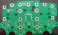
Introduction to Heavy Copper PCB
Heavy copper PCB, also known as thick copper PCB or high current PCB, is a type of printed circuit board that uses thicker copper traces than standard PCBs. These boards are designed to handle higher currents and power levels, making them ideal for applications that require high power delivery or heat dissipation. The increased copper thickness allows for better electrical conductivity and thermal management, which are critical factors in many industrial and automotive applications.
Copper Thickness in Heavy Copper PCBs
The copper thickness in a standard PCB typically ranges from 1 oz to 2 oz per square foot (35-70 μm). In contrast, heavy copper PCBs can have copper thicknesses ranging from 3 oz to 20 oz per square foot (105-700 μm) or even higher in some cases. The exact thickness required depends on the specific application and the amount of current the board needs to carry.
| Copper Weight (oz/ft²) | Copper Thickness (μm) |
|---|---|
| 1 | 35 |
| 2 | 70 |
| 3 | 105 |
| 4 | 140 |
| 6 | 210 |
| 8 | 280 |
| 10 | 350 |
| 12 | 420 |
| 16 | 560 |
| 20 | 700 |
Benefits of Heavy Copper PCBs
Increased Current Carrying Capacity
The primary benefit of using a heavy copper PCB is its increased current carrying capacity. Thicker copper traces can handle higher currents without overheating or suffering from voltage drops. This is particularly important in power electronics, where high currents are common.
Improved Heat Dissipation
Heavy copper PCBs also offer better heat dissipation compared to standard PCBs. The increased copper thickness allows for more efficient heat transfer away from components, reducing the risk of thermal damage and improving overall system reliability.
Enhanced Mechanical Strength
The thicker copper layers in heavy copper PCBs provide additional mechanical strength to the board. This can be beneficial in applications where the PCB is subject to physical stress or vibration.
Applications of Heavy Copper PCB
Power Electronics
Heavy copper PCBs are widely used in power electronics applications, such as power supplies, inverters, and motor drives. These applications often require high current handling capabilities and efficient heat dissipation, making heavy copper PCBs an ideal choice.
Automotive Electronics
In the automotive industry, heavy copper PCBs are used in various applications, including:
- Electric vehicle battery management systems
- High-power lighting systems
- Engine control units
- Power distribution modules
The harsh environmental conditions and high power requirements in automotive applications make heavy copper PCBs a necessary component for reliable operation.
Industrial Controls
Industrial control systems, such as programmable logic controllers (PLCs) and motor controllers, often utilize heavy copper PCBs. These boards can handle the high currents and power levels required in industrial settings while providing robust performance and longevity.
Renewable Energy Systems
Heavy copper PCBs are employed in renewable energy systems, such as solar inverters and wind turbine generators. These applications demand high power handling capabilities and reliable operation under varying environmental conditions.

Design Considerations for Heavy Copper PCB
Copper Thickness Selection
Choosing the appropriate copper thickness for a heavy copper PCB depends on several factors, including:
- Current requirements
- Power dissipation needs
- Thermal management considerations
- Manufacturing capabilities
It is essential to carefully calculate the required copper thickness based on these factors to ensure optimal performance and reliability.
Trace Width and Spacing
When designing heavy copper PCBs, trace width and spacing must be considered to accommodate the increased copper thickness. Wider traces may be necessary to handle higher currents, while adequate spacing between traces is crucial to prevent short circuits and ensure proper insulation.
Thermal Management
Effective thermal management is critical in heavy copper PCB design. In addition to the inherent heat dissipation benefits of thicker copper, designers may need to incorporate additional features such as thermal vias, heat sinks, or active cooling solutions to further enhance thermal performance.
Manufacturing Challenges
Manufacturing heavy copper PCBs presents some unique challenges compared to standard PCBs. The increased copper thickness can impact drilling, etching, and plating processes, requiring specialized equipment and expertise. It is important to work with a PCB manufacturer experienced in heavy copper PCB fabrication to ensure the best results.

FAQs
1. What is the difference between heavy copper PCB and standard PCB?
The main difference between heavy copper PCB and standard PCB lies in the thickness of the copper traces. Heavy copper PCBs use thicker copper, typically ranging from 3 oz to 20 oz per square foot, while standard PCBs use copper thicknesses of 1 oz to 2 oz per square foot.
2. What are the advantages of using heavy copper PCB?
The advantages of using heavy copper PCB include increased current carrying capacity, improved heat dissipation, and enhanced mechanical strength. These benefits make heavy copper PCBs suitable for applications that require high power delivery, efficient thermal management, and robust performance.
3. In what industries are heavy copper PCBs commonly used?
Heavy copper PCBs are commonly used in industries such as power electronics, automotive electronics, industrial controls, and renewable energy systems. These industries often require high power handling capabilities and reliable operation under demanding conditions.
4. How do I select the appropriate copper thickness for my heavy copper PCB design?
Selecting the appropriate copper thickness for a heavy copper PCB design involves considering factors such as current requirements, power dissipation needs, thermal management considerations, and manufacturing capabilities. It is essential to carefully calculate the required copper thickness based on these factors to ensure optimal performance and reliability.
5. Are there any manufacturing challenges associated with heavy copper PCBs?
Yes, manufacturing heavy copper PCBs can present some challenges compared to standard PCBs. The increased copper thickness can impact drilling, etching, and plating processes, requiring specialized equipment and expertise. It is important to work with a PCB manufacturer experienced in heavy copper PCB fabrication to ensure the best results.

Conclusion
Heavy copper PCBs offer numerous benefits over standard PCBs, including increased current carrying capacity, improved heat dissipation, and enhanced mechanical strength. These advantages make them ideal for applications in power electronics, automotive electronics, industrial controls, and renewable energy systems. When designing heavy copper PCBs, careful consideration must be given to copper thickness selection, trace width and spacing, thermal management, and manufacturing challenges. By understanding the unique characteristics and requirements of heavy copper PCBs, designers can create robust and reliable solutions for demanding high-power applications.
Leave a Reply