Introduction to PCB Simulation
Printed circuit board (PCB) simulation is an essential part of the PCB design process. It allows engineers to virtually test and validate the performance, signal integrity, power integrity, and electromagnetic compatibility of a PCB design before physically manufacturing the board.
There are two main types of PCB simulation:
1. Pre-layout simulation
2. Post-layout simulation
Understanding the differences between pre-layout and post-layout simulation is critical for ensuring a robust, reliable, and manufacturable PCB design. In this article, we’ll dive deep into pre-layout vs post-layout simulation, explain the benefits and limitations of each, and discuss when to use them in the PCB design workflow.
What is Pre-Layout PCB Simulation?
Pre-layout PCB simulation, also known as schematic-based simulation, is performed early in the design process before the physical PCB layout is created. It uses the schematic diagram of the circuit to analyze and simulate the ideal behavior of the design.
Goals of Pre-Layout Simulation
The primary goals of pre-layout simulation are to:
- Verify the logical correctness of the circuit
- Optimize component values and parameters
- Assess the theoretical performance of the design
- Identify potential issues early in the design cycle
By simulating the circuit at the schematic level, engineers can quickly iterate and refine the design without investing time in the physical layout.
Pre-Layout Simulation Techniques
Several simulation techniques are commonly used in pre-layout analysis:
| Technique | Description |
|---|---|
| DC Analysis | Calculates the steady-state voltages and currents in the circuit |
| AC Analysis | Evaluates the frequency response, gain, and phase of the circuit |
| Transient Analysis | Simulates the time-domain behavior of the circuit under dynamic conditions |
| Monte Carlo Analysis | Assesses the impact of component tolerances and variations on circuit performance |
These techniques help engineers characterize the ideal behavior of the circuit and identify potential issues related to component selection, biasing, and signal integrity.
Benefits of Pre-Layout Simulation
Pre-layout simulation offers several benefits:
- Quick design iteration and optimization
- Early detection of design flaws and errors
- Reduced design time and cost
- Improved communication between schematic and layout designers
By identifying and resolving issues at the schematic level, pre-layout simulation can significantly streamline the PCB design process and reduce the risk of costly redesigns.
Limitations of Pre-Layout Simulation
While pre-layout simulation is valuable, it has some limitations:
- Ideal component models may not accurately represent real-world behavior
- Does not account for physical layout effects (e.g., trace impedance, crosstalk, parasitic)
- Limited ability to analyze power and signal integrity issues
To address these limitations and gain a more accurate understanding of the PCB’s performance, post-layout simulation is necessary.

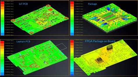
What is Post-Layout PCB Simulation?
Post-layout PCB simulation, also known as layout-based simulation, is performed after the physical PCB layout is created. It takes into account the actual physical characteristics of the PCB, including trace geometry, layer stackup, and component placement.
Goals of Post-Layout Simulation
The primary goals of post-layout simulation are to:
- Verify the performance of the PCB design in the real world
- Identify and resolve signal and power integrity issues
- Assess the impact of the physical layout on circuit behavior
- Ensure the design meets electromagnetic compatibility (EMC) requirements
By simulating the PCB layout, engineers can gain a more accurate understanding of the design’s performance and identify potential issues that may not be apparent in pre-layout simulation.
Post-Layout Simulation Techniques
Several simulation techniques are commonly used in post-layout analysis:
| Technique | Description |
|---|---|
| Signal Integrity Analysis | Evaluates the quality of signals propagating through the PCB traces |
| Power Integrity Analysis | Assesses the power delivery network and identifies voltage drop and noise issues |
| Electromagnetic Compatibility Analysis | Simulates the PCB’s electromagnetic emissions and susceptibility |
| Thermal Analysis | Evaluates the thermal performance of the PCB and identifies hot spots |
These techniques help engineers optimize the physical layout of the PCB to ensure reliable performance and compliance with industry standards.
Benefits of Post-Layout Simulation
Post-layout simulation offers several benefits:
- Accurate modeling of real-world PCB behavior
- Identification and resolution of signal and power integrity issues
- Verification of EMC compliance
- Improved reliability and manufacturability of the PCB design
By simulating the actual physical layout of the PCB, post-layout simulation provides a more comprehensive and accurate assessment of the design’s performance.
Limitations of Post-Layout Simulation
While post-layout simulation is essential for ensuring a robust PCB design, it has some limitations:
- Requires a complete PCB layout, which can be time-consuming to create
- Simulation results may be sensitive to the accuracy of the PCB model and simulation settings
- May require specialized simulation tools and expertise
Despite these limitations, post-layout simulation is a critical step in the PCB design process and should not be overlooked.

Pre-Layout vs Post-Layout Simulation: When to Use Each
Both pre-layout and post-layout simulation play important roles in the PCB design process. The choice between the two depends on the stage of the design and the specific goals of the simulation.
When to Use Pre-Layout Simulation
Pre-layout simulation is most effective in the early stages of the design process when the schematic is being developed and refined. It is particularly useful for:
- Verifying the logical correctness of the circuit
- Optimizing component values and parameters
- Assessing the theoretical performance of the design
- Identifying potential issues early in the design cycle
By performing pre-layout simulation, engineers can quickly iterate and refine the design at the schematic level, saving time and effort in the long run.
When to Use Post-Layout Simulation
Post-layout simulation is essential in the later stages of the design process, after the physical PCB layout has been created. It is particularly useful for:
- Verifying the performance of the PCB design in the real world
- Identifying and resolving signal and power integrity issues
- Assessing the impact of the physical layout on circuit behavior
- Ensuring the design meets electromagnetic compatibility (EMC) requirements
By performing post-layout simulation, engineers can ensure that the PCB design will perform as expected in the real world and meet all necessary performance and regulatory requirements.
Combining Pre-Layout and Post-Layout Simulation
In practice, the most effective approach is to use both pre-layout and post-layout simulation in a complementary manner. Pre-layout simulation can be used to quickly refine the schematic and identify potential issues early on, while post-layout simulation can be used to verify the performance of the final PCB design and ensure its manufacturability.

FAQ
1. What is the main difference between pre-layout and post-layout PCB simulation?
The main difference between pre-layout and post-layout PCB simulation is that pre-layout simulation is performed on the schematic diagram before the physical PCB layout is created, while post-layout simulation is performed on the actual physical layout of the PCB.
2. Can I skip pre-layout simulation and only perform post-layout simulation?
While it is possible to skip pre-layout simulation and only perform post-layout simulation, it is not recommended. Pre-layout simulation is important for quickly refining the schematic and identifying potential issues early in the design process, which can save time and effort in the long run.
3. What are the benefits of performing both pre-layout and post-layout simulation?
Performing both pre-layout and post-layout simulation provides a comprehensive assessment of the PCB design’s performance. Pre-layout simulation helps optimize the schematic and identify potential issues early on, while post-layout simulation verifies the performance of the final PCB design and ensures its manufacturability.
4. What simulation techniques are commonly used in pre-layout and post-layout analysis?
Common pre-layout simulation techniques include DC analysis, AC analysis, transient analysis, and Monte Carlo analysis. Common post-layout simulation techniques include signal integrity analysis, power integrity analysis, electromagnetic compatibility analysis, and thermal analysis.
5. How can I ensure the accuracy of my post-layout simulation results?
To ensure the accuracy of post-layout simulation results, it is important to use accurate PCB models and simulation settings. This may require specialized simulation tools and expertise. It is also important to validate simulation results against actual measurements whenever possible.
Conclusion
PCB simulation is a critical aspect of the PCB design process, enabling engineers to virtually test and validate the performance of a design before physically manufacturing the board. Pre-layout and post-layout simulation are two essential types of PCB simulation, each with its own benefits and limitations.
Pre-layout simulation is performed on the schematic diagram and is useful for quickly refining the design and identifying potential issues early in the process. Post-layout simulation, on the other hand, is performed on the actual physical layout of the PCB and provides a more accurate assessment of the design’s real-world performance.
To ensure a robust, reliable, and manufacturable PCB design, it is important to use both pre-layout and post-layout simulation in a complementary manner. By leveraging the strengths of each type of simulation, engineers can optimize the design at the schematic level, verify its performance in the real world, and ensure compliance with all necessary performance and regulatory requirements.
Leave a Reply