Introduction to Solder Mask
Solder mask, also known as solder resist or solder stop, is a crucial component in the manufacturing of printed circuit boards (PCBs). It is a thin, protective layer applied to the copper traces of a PCB to prevent solder from adhering to undesired areas during the soldering process. Solder mask serves multiple purposes, including protecting the copper traces from oxidation, preventing short circuits, and providing a more aesthetically pleasing appearance to the finished PCB.
Types of Solder Mask
There are two main types of solder mask used in PCB manufacturing:
- Liquid Photoimageable Solder Mask (LPISM)
- Dry Film Solder Mask (DFSM)
Liquid Photoimageable Solder Mask (LPISM)
LPISM is the most common type of solder mask used in the PCB Industry. It is applied as a liquid coating and then exposed to UV light through a photomask, which hardens the exposed areas. The unexposed areas are then removed during the development process, leaving the desired solder mask pattern on the PCB.
Advantages of LPISM:
– High resolution and accuracy
– Excellent adhesion to the PCB surface
– Suitable for complex designs and fine-pitch components
– Wide range of color options available
Dry Film Solder Mask (DFSM)
DFSM is a solid film that is laminated onto the PCB surface using heat and pressure. It is then exposed to UV light through a photomask, which polymerizes the exposed areas. The unexposed areas are removed during the development process, leaving the desired solder mask pattern on the PCB.
Advantages of DFSM:
– Faster application process compared to LPISM
– Consistent thickness across the entire PCB
– Suitable for high-volume production
– Less expensive than LPISM for large quantities
Properties and Characteristics of Solder Mask
Solder mask possesses several key properties and characteristics that make it an essential component in PCB manufacturing:
-
Insulation: Solder mask acts as an insulator, preventing short circuits between adjacent copper traces and components.
-
Protection: It protects the copper traces from oxidation, scratches, and other environmental factors that could damage the PCB.
-
Solderability: Solder mask is designed to have a high resistance to molten solder, ensuring that solder only adheres to the exposed metal surfaces (pads and vias) during the soldering process.
-
Adhesion: A good solder mask must have excellent adhesion to the PCB surface to prevent delamination or peeling during the manufacturing process and throughout the lifespan of the PCB.
-
Thermal stability: Solder mask should be able to withstand the high temperatures involved in the soldering process without degrading or losing its properties.
-
Flame retardancy: Many solder masks are formulated to be flame retardant, which helps prevent the spread of fire in case of a PCB malfunction or external fire.
-
Color options: Solder mask is available in a variety of colors, with green being the most common. Other colors include red, blue, yellow, black, and white. The choice of color can be based on aesthetic preferences, industry standards, or for functional purposes, such as improving contrast for better visual inspection.

Solder Mask Application Process
The application of solder mask involves several steps:
-
Surface preparation: The PCB surface is cleaned to remove any contaminants, and a surface roughening process (such as brushing or chemical etching) is performed to improve solder mask adhesion.
-
Solder mask application: The chosen type of solder mask (LPISM or DFSM) is applied to the PCB surface. LPISM is typically applied using screen printing or spraying, while DFSM is laminated onto the surface using heat and pressure.
-
Exposure: The solder mask-coated PCB is exposed to UV light through a photomask, which hardens or polymerizes the exposed areas. The photomask contains the desired solder mask pattern, allowing UV light to pass through only in the areas where the solder mask should be removed.
-
Development: The unexposed areas of the solder mask are removed using a chemical developer solution, leaving the desired solder mask pattern on the PCB.
-
Curing: The PCB is then subjected to a high-temperature curing process to fully harden the solder mask and improve its mechanical and chemical properties.
-
Inspection: The finished PCB undergoes a visual inspection to ensure that the solder mask is correctly applied and free from defects such as pinholes, blisters, or misalignment.

Solder Mask Design Considerations
When designing a PCB, there are several factors to consider regarding solder mask:
-
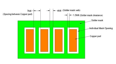
Solder mask clearance: It is essential to maintain a sufficient clearance between the solder mask and the exposed metal surfaces (pads and vias) to ensure proper solderability. The clearance should be large enough to accommodate the tolerances of the solder mask application process.
-
Solder mask sliver: Solder mask slivers, which are thin strips of solder mask between closely spaced pads or traces, should be avoided or minimized. If the slivers are too thin, they may break off during the manufacturing process or in the field, leading to short circuits.
-
Solder mask bridge: A solder mask bridge is an unintentional connection of solder mask between two adjacent pads or traces. This can happen if the spacing between the pads or traces is too small or if the solder mask application process is not well-controlled. Solder mask bridges can cause short circuits and should be avoided.
-
Solder mask dam: A solder mask dam is a intentional widening of the solder mask between two adjacent pads or traces to prevent solder bridging during the soldering process. This is especially important for fine-pitch components or in areas where the risk of solder bridging is high.
-
Legend and marking: The solder mask layer can also be used to apply legends and markings to the PCB, such as component outlines, pin numbers, and polarity indicators. These markings should be clearly visible and legible to facilitate assembly and troubleshooting.

Comparing Solder Mask to Other PCB Coatings
In addition to solder mask, there are other coatings and finishes that can be applied to PCBs for protection and functionality:
-
Conformal coating: A thin, protective polymer film that conforms to the contours of the PCB and its components. It provides additional protection against moisture, dust, chemicals, and mechanical stress. Conformal coating is typically applied after the soldering process and is used in environments where the PCB is exposed to harsh conditions.
-
Hard gold plating: A layer of gold plated onto the exposed metal surfaces of the PCB, such as edge connectors or test points. Hard gold plating provides excellent corrosion resistance, wear resistance, and electrical conductivity. It is commonly used in high-reliability applications or where frequent mating and unmating of connectors is required.
-
Immersion silver (IAg) and immersion tin (ISn): These are surface finishes applied to the exposed metal surfaces of the PCB to protect against oxidation and improve solderability. IAg and ISn are less expensive alternatives to hard gold plating and are suitable for most standard PCB applications.
Comparison table:
| Coating/Finish | Purpose | Application | Advantages | Disadvantages |
|---|---|---|---|---|
| Solder Mask | Insulation, protection, solderability | Applied before soldering | High resolution, excellent adhesion, various colors | Requires UV exposure and development |
| Conformal Coating | Additional protection against moisture, dust, chemicals, and mechanical stress | Applied after soldering | Conforms to PCB contours, provides extra protection | Can be difficult to remove for rework or repair |
| Hard Gold Plating | Corrosion resistance, wear resistance, electrical conductivity | Applied to specific areas (e.g., edge connectors, test points) | Excellent durability and conductivity | Expensive, requires additional processing steps |
| Immersion Silver (IAg) and Immersion Tin (ISn) | Protection against oxidation, improved solderability | Applied to exposed metal surfaces | Less expensive than hard gold plating, suitable for most applications | Not as durable as hard gold plating |
Frequently Asked Questions (FAQ)
-
Q: What is the difference between solder mask and conformal coating?
A: Solder mask is applied before the soldering process and serves to protect the copper traces, prevent solder from adhering to undesired areas, and provide insulation. Conformal coating is applied after the soldering process and provides additional protection against moisture, dust, chemicals, and mechanical stress. -
Q: Can solder mask be removed for rework or repair?
A: Yes, solder mask can be removed using various methods such as mechanical abrasion, chemical etching, or laser ablation. However, care must be taken not to damage the underlying copper traces or components during the removal process. -
Q: What is the most common color for solder mask?
A: Green is the most common color for solder mask, but other colors such as red, blue, yellow, black, and white are also available. The choice of color can be based on aesthetic preferences, industry standards, or for functional purposes, such as improving contrast for better visual inspection. -
Q: How does solder mask affect the impedance of PCB traces?
A: Solder mask has a dielectric constant that can affect the impedance of PCB traces. The thickness and dielectric constant of the solder mask must be taken into account when designing high-speed or impedance-controlled circuits to ensure proper signal integrity. -
Q: Can solder mask be applied to flexible PCBs?
A: Yes, solder mask can be applied to flexible PCBs, but the choice of solder mask material and application process may differ from rigid PCBs. Flexible solder masks, such as polyimide-based materials, are commonly used for flex PCBs to provide the necessary flexibility and durability.
Conclusion
Solder mask is a vital component in the manufacturing of printed circuit boards, providing insulation, protection, and solderability to the copper traces. Understanding the types, properties, and application process of solder mask is essential for designing and manufacturing high-quality, reliable PCBs. By considering factors such as solder mask clearance, sliver, bridge, and dam, as well as the choice of color and compatibility with other PCB coatings and finishes, designers and manufacturers can ensure optimal performance and longevity of their PCBs.
As PCB technology continues to advance, with increasing complexity and miniaturization, the role of solder mask in ensuring proper functionality and reliability becomes even more critical. Staying up-to-date with the latest developments in solder mask materials, application techniques, and design guidelines is crucial for professionals in the electronics industry to meet the ever-growing demands of modern electronic devices.
Leave a Reply