Introduction to Silkscreen PCB
Printed Circuit Boards (PCBs) are essential components in modern electronics. They provide a platform for mounting and connecting various electronic components to create functional circuits. One crucial aspect of PCB design and manufacturing is the silkscreen layer. In this article, we will delve into the concept of silkscreen on PCBs, its purpose, the silkscreen printing process, design considerations, and frequently asked questions.
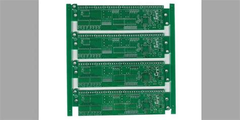
What is a Silkscreen PCB?
A silkscreen PCB refers to a printed circuit board that incorporates a silkscreen layer. The silkscreen layer is a non-conductive ink layer printed on the surface of the PCB. It serves several purposes, including component identification, orientation marking, branding, and providing visual cues for assembly and debugging.
The term “silkscreen” originates from the traditional printing method used to apply the ink layer. However, modern PCB manufacturing often employs advanced printing techniques, such as liquid photo imaging or direct legend printing, to achieve higher precision and resolution.
The Purpose of Silkscreen on PCBs
The silkscreen layer on a PCB serves multiple functions:
-
Component Identification: Silkscreen is used to label components on the PCB, such as resistors, capacitors, integrated circuits (ICs), and connectors. The labels typically include the component’s reference designator (e.g., R1, C2, U3) and sometimes additional information like component values or part numbers. This labeling helps in assembly, troubleshooting, and maintenance of the PCB.
-
Orientation Marking: Silkscreen markings indicate the orientation of components, particularly for polarized components like electrolytic capacitors, diodes, and ICs. Common orientation markings include notches, dots, or lines that align with the component’s pin 1 or cathode. Proper orientation is crucial for correct assembly and preventing damage to components.
-
Branding and Aesthetics: The silkscreen layer can be used to display company logos, product names, version numbers, or other branding elements. This enhances the professional appearance of the PCB and helps in product identification. Silkscreen designs can also incorporate aesthetic elements to improve the visual appeal of the PCB.
-
Assembly and Debug Information: Silkscreen can provide additional information to aid in PCB Assembly and debugging. This may include labels for connectors, test points, switch positions, LED indicators, or debug interfaces. Clear and informative silkscreen markings can greatly simplify the assembly process and assist in troubleshooting efforts.
The Silkscreen Printing Process
The silkscreen printing process involves applying ink to the PCB surface through a patterned mesh or stencil. Here’s a step-by-step overview of the process:
-
Artwork Preparation: The silkscreen artwork is created using PCB design software. The artwork includes all the desired text, labels, and graphics to be printed on the PCB. The artwork is typically generated in a vector format, such as Gerber or EPS, to ensure high-quality printing.
-
Screen Preparation: A fine mesh screen, usually made of polyester or stainless steel, is coated with a light-sensitive emulsion. The prepared artwork is then placed on the screen, and the screen is exposed to light. The areas of the emulsion exposed to light harden, while the unexposed areas remain soluble.
-
Screen Washing: After exposure, the screen is washed with water, removing the soluble emulsion areas. This creates a stencil on the screen, allowing ink to pass through the open areas corresponding to the silkscreen artwork.
-
Ink Application: The PCB is placed beneath the screen, and ink is applied to the screen’s surface. A squeegee is used to press the ink through the open areas of the screen onto the PCB surface. The ink is typically a non-conductive epoxy or UV-curable material.
-
Curing: After printing, the ink is cured to ensure its adhesion to the PCB surface. Curing methods vary depending on the type of ink used. Some inks require air drying, while others need exposure to ultraviolet (UV) light or heat for proper curing.
-
Inspection: Once the ink is cured, the PCB undergoes a visual inspection to ensure the quality and accuracy of the silkscreen printing. Any defects or inconsistencies are identified and corrected if necessary.
| Step | Process | Description |
|---|---|---|
| 1 | Artwork Preparation | Create silkscreen artwork using PCB design software |
| 2 | Screen Preparation | Coat mesh screen with light-sensitive emulsion and expose with artwork |
| 3 | Screen Washing | Wash screen to remove soluble emulsion and create stencil |
| 4 | Ink Application | Apply ink to screen and press through onto PCB surface using squeegee |
| 5 | Curing | Cure ink using air drying, UV light, or heat to ensure adhesion |
| 6 | Inspection | Visually inspect silkscreen printing for quality and accuracy |

Silkscreen Design Considerations
When designing the silkscreen layer for a PCB, several considerations should be taken into account to ensure legibility, clarity, and manufacturability:
Font Selection and Size
Choose a font that is clear, legible, and suitable for small sizes. Sans-serif fonts like Arial, Helvetica, or Verdana are commonly used due to their simplicity and readability. The font size should be appropriate for the available space on the PCB and the intended viewing distance. A minimum font size of 0.8mm (0.032 inches) is generally recommended for good legibility.
Spacing and Placement
Ensure adequate spacing between silkscreen elements to avoid crowding and improve readability. Maintain a minimum clearance of 0.25mm (0.010 inches) between silkscreen and exposed copper features, such as pads and traces. Place silkscreen markings in a way that does not obstruct important components or interfere with the assembly process.
Color and Contrast
The most common color for silkscreen is white, as it provides good contrast against the typical green or black PCB Substrate. However, other colors like black, yellow, or red can be used for specific purposes or to enhance visual appeal. Ensure sufficient contrast between the silkscreen color and the PCB substrate to maintain legibility.
Orientation and Alignment
Orient silkscreen text and graphics in a consistent and logical manner. Text should be aligned horizontally or vertically for easy reading. Use appropriate orientation markings for polarized components, such as a notch or dot at the pin 1 location. Align silkscreen elements with the component outlines or pads for clear association.
Acronyms and Abbreviations
When space is limited, acronyms and abbreviations can be used to conserve real estate on the PCB. However, ensure that the abbreviations are commonly understood and unambiguous. Provide a legend or reference document that explains the meaning of any non-standard acronyms or abbreviations used in the silkscreen.

Frequently Asked Questions (FAQ)
1. Can silkscreen be applied to both sides of a PCB?
Yes, silkscreen can be applied to both the top and bottom sides of a PCB. This is particularly useful for double-sided PCBs where components are mounted on both sides. However, keep in mind that the silkscreen on the bottom side will be mirrored compared to the top side.
2. Is silkscreen necessary for every PCB?
While silkscreen is highly recommended for most PCBs, it is not always necessary. Simple PCBs with few components or those intended for personal projects may forgo the silkscreen layer to save costs. However, for professional production and complex PCBs, silkscreen is essential for assembly, debugging, and maintainability.
3. Can silkscreen be used for Solder mask purposes?
No, silkscreen is not suitable for solder mask purposes. Solder mask is a separate layer applied to the PCB to protect the copper traces and prevent solder bridging. Silkscreen ink is non-conductive and does not provide the necessary insulation and protection offered by solder mask.
4. How durable is the silkscreen on a PCB?
The durability of silkscreen depends on the ink material and the curing process used. Properly cured silkscreen is resistant to abrasion, chemicals, and humidity. However, excessive handling, scratching, or exposure to harsh environments can degrade the silkscreen over time. Conformal coating can be applied over the silkscreen for added protection in demanding applications.
5. Can silkscreen be customized with logos or graphics?
Yes, silkscreen can be customized with logos, graphics, or any desired artwork. PCB design software allows for the creation of custom silkscreen elements. However, ensure that the artwork is compatible with the silkscreen printing process and follows the design guidelines for minimum line width and spacing.

Conclusion
Silkscreen is a vital element in PCB design and manufacturing. It serves multiple purposes, including component identification, orientation marking, branding, and providing assembly and debug information. The silkscreen printing process involves creating a stencil on a mesh screen and applying ink to the PCB surface through the screen.
When designing the silkscreen layer, consider factors such as font selection, size, spacing, color contrast, and orientation to ensure legibility and clarity. Silkscreen can be applied to both sides of the PCB and can be customized with logos and graphics.
While silkscreen is not essential for every PCB, it is highly recommended for professional production and complex designs. It enhances the manufacturability, assembly, and maintainability of the PCB.
By understanding the importance and process of silkscreen on PCBs, designers and manufacturers can create high-quality and user-friendly circuit boards that meet the demands of modern electronics.
Leave a Reply