Introduction to Solder Mask
Solder mask, also known as solder resist or solder stop mask, is a thin layer of polymer that is applied to the surface of a printed circuit board (PCB) to protect the copper traces from oxidation and to prevent solder bridges from forming during the soldering process. It is a crucial component in the manufacturing of PCBs, as it ensures the reliability and functionality of the electronic device.
What is a Printed Circuit Board (PCB)?
A printed circuit board is a flat board made of insulating material, such as fiberglass or plastic, with conductive copper traces printed on its surface. These traces connect the various electronic components, such as resistors, capacitors, and integrated circuits, to form a complete electronic circuit. PCBs are used in almost all electronic devices, from smartphones and computers to medical equipment and aerospace systems.
The Role of Solder Mask in PCB Manufacturing
Solder mask plays a critical role in the manufacturing of PCBs by providing several benefits:
-
Protection from Oxidation: Copper traces on a PCB can easily oxidize when exposed to air, which can lead to reduced conductivity and poor performance. Solder mask acts as a barrier between the copper traces and the environment, preventing oxidation and ensuring the long-term reliability of the PCB.
-
Prevention of Solder Bridges: During the soldering process, molten solder can sometimes flow between adjacent copper traces, creating unwanted electrical connections known as solder bridges. Solder mask covers the areas between the traces, preventing solder from flowing where it shouldn’t and minimizing the risk of short circuits.
-
Improved Aesthetics: Solder mask is available in various colors, with green being the most common. The color of the solder mask can enhance the visual appeal of the PCB and make it easier to identify components and traces.
-
Increased Durability: Solder mask provides an additional layer of protection to the PCB, making it more resistant to scratches, abrasions, and other forms of mechanical damage.
Types of Solder Mask
There are two main types of solder mask: liquid photoimageable (LPI) and dry film photoimageable (DFPI).
Liquid Photoimageable (LPI) Solder Mask
LPI solder mask is the most common type used in PCB manufacturing. It is applied to the PCB as a liquid and then exposed to ultraviolet (UV) light through a photomask, which hardens the exposed areas. The unexposed areas are then removed using a developer solution, leaving behind the desired solder mask pattern.
Advantages of LPI solder mask include:
- High resolution and accuracy
- Ability to cover fine details and small features
- Excellent adhesion to the PCB surface
- Smooth and even surface finish
Dry Film Photoimageable (DFPI) Solder Mask
DFPI solder mask is applied to the PCB as a dry film and then exposed to UV light through a photomask, similar to the LPI process. The unexposed areas are removed using a developer solution, leaving behind the desired solder mask pattern.
Advantages of DFPI solder mask include:
- Faster application process compared to LPI
- More cost-effective for high-volume production
- Good resistance to chemicals and solvents
- Suitable for both rigid and Flexible PCBs

Solder Mask Application Process
The solder mask application process typically involves the following steps:
-
Surface Preparation: The PCB surface is cleaned and prepared to ensure proper adhesion of the solder mask.
-
Solder Mask Application: The solder mask is applied to the PCB surface using either the LPI or DFPI method.
-
Exposure: The solder mask is exposed to UV light through a photomask, which hardens the exposed areas.
-
Development: The unexposed areas of the solder mask are removed using a developer solution, leaving behind the desired solder mask pattern.
-
Curing: The PCB is heated to fully cure the solder mask and ensure its durability and resistance to environmental factors.
-
Inspection: The PCB is inspected for any defects or imperfections in the solder mask, such as pinholes, bubbles, or incomplete coverage.

Solder Mask Design Considerations
When designing a PCB, several factors must be considered to ensure the proper application and performance of the solder mask:
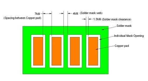
Solder Mask Clearance
Solder mask clearance refers to the distance between the edge of a copper pad or trace and the edge of the solder mask opening. Adequate clearance is necessary to ensure proper soldering and to prevent solder bridging. The amount of clearance required depends on the size of the pad or trace and the soldering process used.
| Pad/Trace Size | Recommended Solder Mask Clearance |
|---|---|
| < 0.5 mm | 0.1 mm |
| 0.5 – 1.0 mm | 0.15 mm |
| > 1.0 mm | 0.2 mm |
Solder Mask Thickness
The thickness of the solder mask can affect its performance and durability. A thicker solder mask provides better protection against oxidation and mechanical damage, but may also reduce the resolution and accuracy of the PCB features. The optimal solder mask thickness depends on the specific requirements of the PCB and the manufacturing process used.
| Solder Mask Type | Recommended Thickness |
|---|---|
| LPI | 0.02 – 0.04 mm |
| DFPI | 0.03 – 0.05 mm |
Solder Mask Color
Solder mask is available in various colors, with green being the most common. The choice of color is primarily a matter of aesthetics and personal preference, but it can also affect the PCB’s performance in certain applications. For example, black solder mask is often used in high-temperature applications due to its better heat absorption properties.
Solder Mask Finish
The surface finish of the solder mask can impact its ability to repel moisture and protect the PCB from environmental factors. Common solder mask finishes include:
- Glossy: Provides a smooth, shiny surface that is easy to clean and inspect.
- Matte: Offers a non-reflective surface that can reduce glare and improve the readability of component markings.
- Semi-glossy: A compromise between glossy and matte finishes, providing a balance of aesthetics and functionality.

Frequently Asked Questions (FAQ)
-
What is the difference between solder mask and silkscreen?
Solder mask is a protective layer applied to the PCB to cover the copper traces and prevent solder bridges, while silkscreen is a printed layer on top of the solder mask that contains component labels, logos, and other markings for easier assembly and identification. -
Can solder mask be removed?
Yes, solder mask can be removed using abrasive methods such as sanding or chemical methods such as using a solder mask removal solution. However, removing the solder mask can expose the copper traces to oxidation and other environmental factors, so it should only be done when necessary for repairs or modifications. -
Is solder mask electrically conductive?
No, solder mask is an insulating material and does not conduct electricity. Its primary purpose is to protect the conductive copper traces from oxidation and prevent solder bridges. -
What is the most common color for solder mask?
Green is the most common color for solder mask, but other colors such as blue, red, yellow, black, and white are also available. The choice of color is primarily a matter of aesthetics and personal preference. -
Can solder mask withstand high temperatures?
Yes, most solder masks are designed to withstand the high temperatures associated with the soldering process, typically up to 260°C (500°F). However, prolonged exposure to high temperatures can cause the solder mask to degrade over time, so it is essential to consider the specific requirements of the application when selecting a solder mask.
Conclusion
Solder mask is a critical component in the manufacturing of Printed Circuit Boards, providing protection against oxidation, solder bridging, and mechanical damage. By understanding the types of solder mask, the application process, and the design considerations involved, PCB Designers and manufacturers can ensure the reliability and functionality of their electronic devices. As electronics continue to advance and become more complex, the role of solder mask in PCB manufacturing will remain essential for producing high-quality, reliable products.
Leave a Reply