Introduction to PCB Manufacturing
Printed Circuit Boards (PCBs) are the backbone of modern electronics. They are used in almost every electronic device, from smartphones and computers to medical equipment and aerospace systems. PCBs provide a platform for electronic components to be connected and communicate with each other, enabling complex circuits to be built in a compact and efficient manner.
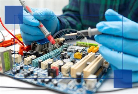
PCB manufacturing is a complex process that involves multiple steps and requires precision and attention to detail. In this article, we will take a deep dive into the PCB manufacturing process, from design to final assembly, and explore the various steps involved in creating high-quality PCBs.
The PCB Manufacturing Process
Step 1: PCB Design
The first step in PCB manufacturing is the design phase. This is where the circuit schematic is created, and the layout of the PCB is determined. The design process typically involves the following steps:
-
Schematic Design: The circuit schematic is created using electronic design automation (EDA) software. The schematic shows the electrical connections between components and helps to ensure that the circuit will function as intended.
-
Component Selection: The components that will be used in the PCB are selected based on the circuit requirements, such as voltage, current, and frequency.
-
PCB Layout: The layout of the PCB is designed using EDA software. The layout determines the placement of components and the routing of traces between them. The layout must take into account factors such as signal integrity, electromagnetic compatibility, and thermal management.
-
Design Rule Check (DRC): The PCB layout is checked against a set of design rules to ensure that it meets manufacturing requirements and will function as intended.
Step 2: PCB Fabrication
Once the PCB design is complete, the next step is fabrication. This is where the physical PCB is created from the digital design files. The fabrication process typically involves the following steps:
-
Creating the Copper Pattern: The first step in PCB fabrication is to create the copper pattern on the PCB substrate. This is typically done using a photolithography process, where a photoresist layer is applied to the substrate and exposed to light through a mask that contains the PCB layout. The exposed areas of the photoresist are then removed, leaving the copper pattern behind.
-
Etching: The next step is to remove the unwanted copper from the substrate, leaving only the desired copper pattern. This is typically done using a chemical etching process, where the PCB is immersed in an etchant solution that dissolves the unwanted copper.
-
Drilling: Holes are drilled in the PCB to allow for the mounting of components and the creation of vias (electrical connections between layers).
-
Plating: The holes and vias are plated with copper to create electrical connections between layers.
-
Solder Mask Application: A solder mask layer is applied to the PCB to protect the copper traces and prevent short circuits.
-
Silkscreen: A silkscreen layer is applied to the PCB to add text and graphics, such as component labels and company logos.
Step 3: PCB Assembly
Once the PCB has been fabricated, the next step is assembly. This is where the electronic components are mounted onto the PCB and soldered in place. The assembly process typically involves the following steps:
-
Solder Paste Application: Solder paste is applied to the PCB pads where components will be mounted. This is typically done using a stencil printing process, where a stencil is placed over the PCB and solder paste is applied through the openings in the stencil.
-
Component Placement: The electronic components are placed onto the PCB using a pick-and-place machine. The machine uses a vacuum nozzle to pick up each component and place it onto the PCB in the correct location.
-
Reflow Soldering: The PCB is heated in a reflow oven to melt the solder paste and create a permanent electrical and mechanical connection between the components and the PCB.
-
Inspection: The assembled PCB is inspected to ensure that all components are properly mounted and soldered. This is typically done using automated optical inspection (AOI) equipment.
-
Functional Testing: The assembled PCB is tested to ensure that it functions as intended. This may involve testing individual components, as well as the overall functionality of the PCB.

Types of PCBs
There are several types of PCBs, each with its own unique characteristics and manufacturing requirements. The most common types of PCBs are:
Single-Layer PCBs
Single-layer PCBs have copper traces on only one side of the substrate. They are the simplest and least expensive type of PCB, but they are limited in terms of circuit complexity and density.
Double-Layer PCBs
Double-layer PCBs have copper traces on both sides of the substrate, with vias connecting the traces on opposite sides. They offer more design flexibility and higher circuit density than single-layer PCBs.
Multi-Layer PCBs
Multi-layer PCBs have multiple layers of copper traces, separated by insulating layers. They offer the highest level of design flexibility and circuit density, but they are also the most complex and expensive to manufacture.
Flexible PCBs
Flexible PCBs are made from flexible materials, such as polyimide, and can be bent or folded to fit into tight spaces. They are commonly used in applications where space is limited or where the PCB needs to conform to a particular shape.
Rigid-Flex PCBs
Rigid-flex PCBs combine the benefits of rigid and flexible PCBs, with rigid sections for mounting components and flexible sections for connecting them. They offer the best of both worlds in terms of design flexibility and reliability.

PCB Materials
The choice of materials used in PCB manufacturing can have a significant impact on the performance and reliability of the finished product. The most common PCB materials are:
FR-4
FR-4 is the most commonly used PCB substrate material. It is a composite material made from woven fiberglass and epoxy resin. FR-4 is strong, durable, and has good electrical insulation properties.
Polyimide
Polyimide is a high-performance polymer that is commonly used in flexible PCBs. It has excellent thermal and mechanical properties, as well as good electrical insulation properties.
Ceramic
Ceramic PCBs are made from alumina or other ceramic materials. They offer excellent thermal conductivity and electrical insulation properties, making them ideal for high-power and high-frequency applications.
Metal Core
Metal core PCBs have a metal substrate, typically aluminum, that provides excellent thermal conductivity. They are commonly used in applications where heat dissipation is a critical factor, such as LED lighting and power electronics.

PCB Surface Finishes
The choice of surface finish can have a significant impact on the solderability, reliability, and environmental resistance of the PCB. The most common PCB surface finishes are:
Hot Air Solder Leveling (HASL)
HASL is the most commonly used PCB surface finish. It involves dipping the PCB in molten solder and then using hot air to level the surface. HASL provides good solderability and is relatively inexpensive, but it can result in an uneven surface and can be prone to defects.
Electroless Nickel Immersion Gold (ENIG)
ENIG involves plating the copper traces with a layer of nickel and then a thin layer of gold. It provides excellent solderability and environmental resistance, but it is more expensive than HASL.
Immersion Silver (IAg)
IAg involves plating the copper traces with a thin layer of silver. It provides good solderability and is less expensive than ENIG, but it is prone to tarnishing over time.
Organic Solderability Preservative (OSP)
OSP involves applying a thin layer of organic compound to the copper traces to prevent oxidation. It provides good solderability and is relatively inexpensive, but it has a limited shelf life and can be prone to defects.
Quality Control in PCB Manufacturing
Quality control is a critical aspect of PCB manufacturing, as defects or failures can have serious consequences in the final application. There are several quality control measures that are commonly used in PCB manufacturing, including:
Visual Inspection
Visual inspection involves examining the PCB for defects or anomalies, such as broken traces, short circuits, or missing components. This is typically done using a microscope or other magnification tool.
Automated Optical Inspection (AOI)
AOI uses cameras and image processing software to automatically inspect the PCB for defects or anomalies. It can detect a wide range of defects, including missing components, incorrect component placement, and solder defects.
X-Ray Inspection
X-ray inspection uses X-rays to examine the internal structure of the PCB, including the solder joints and vias. It can detect defects that are not visible on the surface, such as voids or cracks in the solder joints.
Electrical Testing
Electrical testing involves testing the PCB to ensure that it functions as intended. This may involve testing individual components, as well as the overall functionality of the PCB. Electrical testing can detect a wide range of defects, including short circuits, open circuits, and incorrect component values.
PCB Manufacturing Industry Trends
The PCB manufacturing industry is constantly evolving, driven by advances in technology and changing customer demands. Some of the key trends in the PCB manufacturing industry include:
Miniaturization
As electronic devices become smaller and more complex, PCBs are also becoming smaller and more densely packed. This requires advanced manufacturing techniques, such as high-density interconnect (HDI) PCBs and embedded components.
Increased Demand for High-Frequency PCBs
The growing demand for high-speed data transmission and wireless communication is driving the need for PCBs that can operate at higher frequencies. This requires the use of specialized materials and manufacturing techniques, such as low-loss substrates and controlled impedance routing.
Sustainability and Environmental Responsibility
There is growing pressure on the PCB manufacturing industry to adopt more sustainable and environmentally responsible practices. This includes the use of lead-free solder, the reduction of hazardous chemicals, and the recycling of waste materials.
Automation and Industry 4.0
The PCB manufacturing industry is increasingly adopting automation and Industry 4.0 technologies, such as robotics, machine learning, and the Internet of Things (IoT). These technologies can help to improve efficiency, reduce costs, and enhance quality control.
Frequently Asked Questions (FAQ)
1. What is the typical lead time for PCB manufacturing?
The lead time for PCB manufacturing can vary depending on the complexity of the design, the materials used, and the manufacturer’s workload. Typical lead times range from a few days to several weeks.
2. What is the minimum order quantity for PCBs?
The minimum order quantity for PCBs can vary depending on the manufacturer and the type of PCB. Some manufacturers may have a minimum order quantity of a few pieces, while others may require larger orders of hundreds or thousands of pieces.
3. What is the difference between a prototype PCB and a production PCB?
A prototype PCB is typically used for testing and validation purposes, and may be manufactured using different materials and processes than a production PCB. Production PCBs are manufactured in larger quantities and are designed for use in the final product.
4. Can I design my own PCB?
Yes, it is possible to design your own PCB using electronic design automation (EDA) software. However, it is important to have a good understanding of PCB design principles and manufacturing requirements to ensure that the PCB will function as intended and can be manufactured reliably.
5. How can I ensure the quality of my PCBs?
There are several steps you can take to ensure the quality of your PCBs, including:
- Working with a reputable PCB manufacturer that has a proven track record of quality and reliability.
- Carefully reviewing your PCB design to ensure that it meets all manufacturing requirements and design rules.
- Specifying the appropriate materials and surface finishes for your application.
- Implementing appropriate quality control measures, such as visual inspection, AOI, X-ray inspection, and electrical testing.
- Conducting thorough testing and validation of your PCBs before putting them into production.
Conclusion
PCB manufacturing is a complex and critical process that requires precision, attention to detail, and a deep understanding of the underlying technologies and processes. From design to fabrication to assembly and testing, each step in the PCB manufacturing process plays a crucial role in ensuring the quality, reliability, and functionality of the final product.
As the demands on PCBs continue to evolve, driven by advances in technology and changing customer needs, the PCB manufacturing industry must continue to innovate and adapt. This includes embracing new materials, manufacturing techniques, and quality control measures, as well as adopting more sustainable and environmentally responsible practices.
By understanding the intricacies of the PCB manufacturing process and staying up-to-date with the latest industry trends and best practices, designers, engineers, and manufacturers can work together to create high-quality, reliable, and innovative PCBs that meet the needs of today’s complex electronic systems.
Leave a Reply