Introduction to PCB Stencil
A PCB (Printed Circuit Board) stencil is a thin sheet of material, typically stainless steel or polyester, with laser-cut openings that correspond to the pads on a PCB. The stencil is used to apply solder paste onto the PCB pads before placing components, ensuring precise and consistent solder paste application. This process is crucial for surface mount technology (SMT) assembly, as it enables the accurate placement of small components and helps achieve reliable solder joints.
Types of PCB Stencils
There are two main types of PCB stencils:
-
Stainless Steel Stencils: These stencils are made from high-quality stainless steel and are known for their durability and precision. They are suitable for high-volume production and can withstand repeated use without deformation.
-
Polyester Stencils: Also known as mesh stencils, these are made from a fine polyester mesh coated with a photosensitive emulsion. They are less expensive than stainless steel stencils and are suitable for prototyping or low-volume production.
| Stencil Type | Material | Durability | Precision | Cost | Application |
|---|---|---|---|---|---|
| Stainless Steel | High-quality stainless steel | High | High | Higher | High-volume production |
| Polyester | Fine polyester mesh with photosensitive emulsion | Lower | Moderate | Lower | Prototyping or low-volume production |
How PCB Stencils are Made
Stainless Steel Stencils
-
Design: The stencil design is created using CAD (Computer-Aided Design) software, based on the PCB layout and component specifications.
-
Laser Cutting: A high-precision laser cuts the openings in the stainless steel sheet according to the CAD design. The laser ensures clean, burr-free cuts and maintains the desired aperture size and shape.
-
Cleaning: After laser cutting, the stencil is cleaned to remove any debris or contaminants.
-
Inspection: The stencil undergoes a thorough inspection to ensure that all openings are cut correctly and meet the required specifications.
Polyester Stencils
-
Mesh Preparation: A fine polyester mesh is coated with a photosensitive emulsion and allowed to dry.
-
Exposure: The emulsion-coated mesh is exposed to UV light through a film positive of the stencil design. The exposed areas of the emulsion harden, while the unexposed areas remain soluble.
-
Developing: The unexposed emulsion is washed away, leaving openings in the mesh that correspond to the PCB pads.
-
Drying: The developed stencil is dried, and the remaining emulsion hardens, creating a durable stencil.

Advantages of Using PCB Stencils
-
Precise Solder Paste Application: PCB stencils ensure that the correct amount of solder paste is applied to each pad, resulting in consistent and reliable solder joints.
-
Increased Efficiency: Stencils allow for the rapid application of solder paste to multiple PCBs simultaneously, reducing assembly time and increasing production throughput.
-
Improved Reliability: Consistent solder paste application reduces the risk of defects such as bridging, insufficient solder, or tombstoning, leading to improved overall reliability of the assembled PCBs.
-
Cost Reduction: By minimizing solder paste waste and reducing the need for rework due to defects, PCB stencils help lower overall production costs.

Factors Affecting PCB Stencil Performance
Several factors can impact the performance of a PCB stencil:
-
Aperture Size and Shape: The size and shape of the stencil openings must match the PCB pads and accommodate the solder paste’s particle size. Incorrect aperture dimensions can lead to insufficient or excessive solder paste deposition.
-
Stencil Thickness: The stencil thickness determines the volume of solder paste deposited on the pads. Thicker stencils deposit more paste, while thinner stencils deposit less. The optimal thickness depends on the component size and pitch.
-
Material Quality: High-quality stencil materials ensure durability, precision, and ease of cleaning. Poor-quality materials may lead to premature wear, deformation, or difficulty in achieving consistent solder paste deposition.
-
Cleaning and Maintenance: Regular cleaning and proper maintenance of the stencil are essential to maintain its performance. Solder paste residue can clog apertures, affecting the consistency of paste deposition.

PCB Stencil Design Considerations
When designing a PCB stencil, several factors must be considered:
-
Pad Size and Pitch: The stencil apertures must be sized and spaced according to the PCB pad dimensions and pitch. Smaller pads and finer pitches require more precise stencil design and manufacturing.
-
Solder Paste Properties: The solder paste’s particle size, viscosity, and rheology should be considered when determining the stencil aperture dimensions and thickness.
-
Component Placement: The stencil design must account for the placement of components on the PCB, ensuring that the apertures align with the pads and provide sufficient clearance for the components.
-
Fiducial Marks: Fiducial marks on the stencil help align it with the PCB during the solder paste application process. These marks should be included in the stencil design.
-
Stencil Frame: The stencil frame holds the stencil in place during the printing process. The frame design should be compatible with the solder paste printer and provide adequate support for the stencil.
PCB Stencil Inspection and Quality Control
To ensure the quality and consistency of PCB stencils, regular inspection and quality control measures are necessary:
-
Visual Inspection: Stencils should be visually inspected for any damage, deformation, or clogged apertures. Magnifying lenses or microscopes can be used for detailed examination.
-
Dimensional Verification: The aperture dimensions and positions should be verified using precision measurement tools, such as optical comparators or coordinate measuring machines (CMMs), to ensure they meet the specified tolerances.
-
Solder Paste Volume Measurement: Solder paste volume tests can be performed using specialized equipment to ensure that the stencil deposits the correct amount of paste on the pads.
-
Print Tests: Printing tests on sample PCBs can help evaluate the stencil’s performance in real-world conditions, allowing for any necessary adjustments to be made.
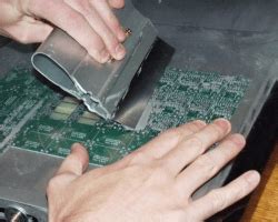
Cleaning and Maintenance of PCB Stencils
Proper cleaning and maintenance of PCB stencils are crucial for ensuring consistent performance and longevity:
-
Regular Cleaning: Stencils should be cleaned regularly to remove solder paste residue and prevent clogging of apertures. Specialized stencil cleaning solutions and equipment are available for this purpose.
-
Gentle Handling: Stencils should be handled gently to avoid damage or deformation. Proper storage and transportation practices help maintain the stencil’s integrity.
-
Inspection and Repair: Regular inspections can identify any damage or wear to the stencil. Minor damage may be repaired using specialized techniques, such as laser welding or electropolishing.
-
Replacement: When a stencil becomes excessively worn or damaged, it should be replaced to ensure consistent solder paste deposition and maintain the quality of the assembled PCBs.
FAQ
-
What is the difference between a stainless steel and polyester PCB stencil?
Stainless steel stencils are more durable, precise, and suitable for high-volume production, while polyester stencils are less expensive and better suited for prototyping or low-volume production. -
How do I choose the right stencil thickness for my PCB?
The optimal stencil thickness depends on the size and pitch of the components on your PCB. Generally, thicker stencils are used for larger components and higher-volume solder paste deposition, while thinner stencils are used for smaller components and finer pitches. -
How often should I clean my PCB stencil?
The frequency of cleaning depends on the volume of production and the type of solder paste used. As a general rule, stencils should be cleaned after every shift or when solder paste buildup becomes visible. Regular cleaning helps prevent aperture clogging and ensures consistent solder paste deposition. -
Can damaged PCB stencils be repaired?
Minor damage to PCB stencils can often be repaired using specialized techniques such as laser welding or electropolishing. However, if the damage is extensive or the stencil is severely worn, it may be more cost-effective to replace the stencil. -
How do I store my PCB stencils when not in use?
PCB stencils should be stored in a clean, dry environment, away from direct sunlight and extreme temperatures. Stainless steel stencils can be stored vertically or horizontally, while polyester stencils should be stored flat to prevent deformation. Proper storage helps extend the life of the stencil and maintains its performance.
Conclusion
PCB stencils play a critical role in the SMT assembly process, ensuring precise and consistent solder paste application. By understanding the types of stencils available, their manufacturing processes, and the factors affecting their performance, engineers and manufacturers can make informed decisions when selecting and using PCB stencils. Proper design, inspection, cleaning, and maintenance of stencils are essential for achieving high-quality, reliable PCB assemblies while minimizing production costs and waste.
As electronics continue to miniaturize and become more complex, the importance of accurate and efficient PCB Assembly processes will only continue to grow. By staying up-to-date with the latest developments in PCB stencil technology and best practices, manufacturers can ensure that their products meet the ever-increasing demands of the market.
Leave a Reply