Why is PCB Edge Plating Important?
There are several key reasons why PCB edge plating is a critical step in PCB manufacturing:
Protection from Environmental Factors
The exposed edges of a PCB are vulnerable to damage from environmental factors like moisture, chemicals, and pollutants. Over time, exposure can lead to corrosion and degradation of the board materials. Edge plating seals and protects the edges to prevent this damage.
Improved Durability
Plated edges are more resistant to chipping, cracking and peeling compared to raw board material. This improves the overall structural integrity and durability of the PCB, allowing it to withstand more wear and tear. Plating is especially important for boards that will be handled frequently or subjected to vibration and impact.
Enhanced Electrical Conductivity
For some PCB Designs, the edges are used to make electrical connections between different layers or to external components. Bare PCB material is not very conductive, so plating the edges with a highly conductive metal like gold ensures a good electrical contact.
Better Shielding Performance
In PCBs designed with shielding to block electromagnetic interference (EMI), plating the edges helps contain the shielding to prevent leakage. Gaps in shielding at the board edges can allow EMI to enter or escape the shielded area, but plating closes off those gaps.
Edge Plating Metals
The two most commonly used metals for PCB edge plating are gold and tin.
Gold Plating
Gold is the preferred choice for high-reliability applications due to its excellent corrosion resistance, electrical conductivity, and durability. Gold-plated edges maintain their integrity and performance for a long time even in harsh operating conditions.
The drawbacks of gold are its high cost and the fact that it is relatively soft, so not as resistant to mechanical wear as some other metals. For this reason, gold is often used for edge connectors and other interfaces where the benefits outweigh the cost.
Tin Plating
Tin is a more economical alternative to gold that still offers good corrosion resistance and conductivity. It is harder than gold, so it holds up better against physical wear and abrasion. Tin is often used for less critical applications where cost is a bigger factor.
The main downside of tin is that it is prone to forming tin whiskers, which are small conductive fibers that can grow out of the plating and cause short circuits. However, this can be mitigated with the addition of a small amount of lead to the plating alloy.

Edge Plating Thickness
The thickness of the plating layer is an important aspect to consider. It affects the mechanical and electrical properties of the plated edge.
Common plating thicknesses used in the PCB industry include:
| Plating Thickness (μm) | Typical Applications |
|---|---|
| 0.05 – 0.5 | Decorative / light corrosion protection |
| 0.5 – 2.0 | Moderate corrosion protection / light wear |
| 2.0 – 5.0 | Heavy corrosion protection / moderate wear |
| 5.0 – 10.0 | Extreme corrosion protection / heavy wear |
| 10.0+ | High-performance electrical contacts and connectors |
Thicker plating provides better protection and wear resistance, but adds more cost and can impact the dimensional tolerances of the board edges. It’s important to choose a plating thickness that balances performance and cost for the intended application.

Edge Plating Methods
There are a few different methods used to apply the plating metal to PCB edges. Each has advantages and limitations.
Electroplating
Electroplating is the most common method for PCB edge plating. It involves immersing the board in a plating solution and using an electric current to deposit metal ions onto the exposed edges.
Advantages of electroplating include:
- Fast and efficient process
- Suitable for high-volume production
- Can plate multiple boards simultaneously
- Produces an even plating thickness
Limitations include:
- Requires additional steps to prepare edges for plating
- Can have issues with coverage in holes and recesses
- Uses hazardous chemicals that require proper handling and disposal
Electroless Plating
Electroless plating is an alternative method that does not require an external electric current. Instead, it uses an autocatalytic chemical reaction to deposit the plating metal.
Advantages of electroless plating include:
- No need for electrical contacts or current source
- Can plate irregularly shaped edges and complex geometries
- Provides more uniform coverage, even in holes and recesses
- Uses less hazardous chemicals than electroplating
Limitations include:
- Slower process than electroplating
- Not as cost-effective for high-volume production
- Limited selection of plating metals
- Can be difficult to control plating thickness
Immersion Plating
Immersion plating is a simple process where the board is dipped into a plating solution and the metal is deposited VIA a displacement reaction. A more active metal in the solution displaces a less active metal on the board surface.
Advantages of immersion plating include:
- Very simple and quick process
- No electrical current or special equipment needed
- Suitable for prototyping and small-scale production
Limitations include:
- Only produces a very thin plating layer
- Limited to certain metal combinations (e.g. gold displacing nickel)
- Poor adhesion and durability compared to other methods
- Can cause unwanted replacement reactions on other board features

Edge Plating Quality Control
Ensuring the quality and consistency of edge plating is critical for PCB reliability. There are several factors that need to be controlled and inspected:
Plating Thickness
The plating thickness must be within the specified tolerances to provide the intended level of protection and performance. Too thin, and it may not be effective; too thick, and it can cause issues with board fit and assembly.
Methods used to measure plating thickness include:
- Cross-sectional analysis
- X-ray fluorescence (XRF) spectroscopy
- Coulometric testing
- Beta backscatter
Adhesion
The plating must adhere strongly to the board edges without peeling or flaking off. Adhesion is typically evaluated using tape tests or peel strength tests that measure the force required to remove the plating.
Coverage and Uniformity
The plating should cover the edges completely and evenly, without any gaps, pinholes or thin spots. Visual inspection is commonly used to check coverage, aided by microscopy for critical applications.
Solderability
If the plated edges will be soldered, they need to have good solderability. This means the surface is wettable by molten solder and can form a strong intermetallic bond. Solderability is assessed using wetting balance tests or solder float tests.
Designing for Edge Plating
When designing a PCB that will have plated edges, there are some best practices to follow to ensure optimal results:
Material Selection
Choose PCB Substrate materials that are compatible with the edge plating process and the operating environment of the finished board. Some materials are more amenable to plating than others.
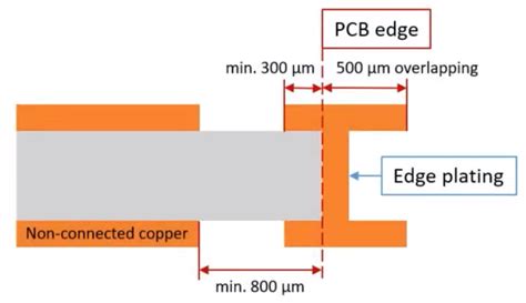
Edge Geometry
Avoid very thin or sharply angled board edges that will be difficult to plate uniformly. Aim for edge thicknesses of at least 0.5 mm for easier plating coverage.
Proximity to Other Features
Provide adequate clearance between the plated edges and any adjacent holes, slots or cutouts. A minimum distance of 2-3 times the plating thickness is recommended to prevent issues with plating buildup or bridging.
Maskability
If the plating needs to be selectively applied to certain areas of the edges, consider using a plating mask or resist. The mask design should account for the plating thickness to ensure proper coverage of the intended areas.
Connector Design
For edge connectors, pay attention to the tolerance stack-up between the plated edge and the mating connector. The plating thickness must be factored in to ensure a good fit and electrical contact.
Frequently Asked Questions
What is the difference between edge plating and surface plating?
Edge plating specifically applies the plating metal to the exposed edges of the PCB, while surface plating applies it to the top and/or bottom surfaces of the board. Edge plating is used for protection and edge connectors, while surface plating is used for solderable finishes, wire bonding, and EMI shielding.
Can PCBs be fabricated with plated edges from the start?
Yes, PCBs can be manufactured with the edges already plated as part of the fabrication process. This involves either pattern plating the edges before the board is cut out, or plating the entire panel and then cutting it into individual boards. However, it’s more common to fabricate the bare boards first and then plate the edges as a separate post-processing step.
How does edge plating affect PCB cost?
Edge plating adds cost to the PCB due to the additional materials and processing steps involved. The type and thickness of the plating metal are the biggest cost factors. Gold is more expensive than tin, and thicker plating requires more material and time. However, the added cost is often justified by the improved protection and performance that plating provides.
Can edge plating be repaired?
Minor damage to edge plating can sometimes be repaired by selectively re-plating the affected area. However, this is not always possible or practical, especially for severe damage or large areas. In many cases, it’s better to replace the board entirely to ensure reliability. Proper handling and storage procedures should be used to minimize the risk of plating damage.
Is edge plating always necessary?
No, edge plating is not required for every PCB application. It is most commonly used for boards that will be exposed to harsh environments, frequently handled, or used in high-reliability applications. For simpler, low-cost consumer electronics, the added expense of edge plating may not be necessary. It’s up to the designer to weigh the costs and benefits for their specific application.
Leave a Reply