Introduction to Copper PCB
Printed Circuit Boards (PCBs) are the backbone of modern electronics, providing a platform for interconnecting electronic components in a compact and efficient manner. Among the various materials used in PCB fabrication, copper stands out as the most commonly used conductor due to its excellent electrical and thermal properties. Copper based PCBs have become the industry standard, offering reliable performance and cost-effectiveness across a wide range of applications.
In this comprehensive article, we will delve into the world of copper based PCBs, exploring their properties, manufacturing processes, advantages, and applications. By the end of this article, you will have a thorough understanding of what copper based PCBs are and why they are so widely used in the electronics industry.
The Role of Copper in PCBs
Electrical Conductivity
Copper is an excellent electrical conductor, making it an ideal choice for PCB traces and pads. Its high conductivity allows for efficient current flow, minimizing resistance and power loss. This property is crucial for maintaining signal integrity and ensuring reliable performance of electronic circuits.
Thermal Conductivity
In addition to its electrical properties, copper also exhibits excellent thermal conductivity. This means that it can effectively dissipate heat generated by electronic components, preventing overheating and thermal damage. Copper’s thermal conductivity helps in maintaining stable operating temperatures, enhancing the overall reliability and longevity of PCBs.
Mechanical Strength
Copper provides mechanical strength to the PCB structure. Its ductility and malleability allow for easy shaping and forming during the manufacturing process. At the same time, copper’s tensile strength ensures that the PCB can withstand physical stresses and vibrations encountered during assembly and operation.

Copper PCB Manufacturing Process
Substrate Preparation
The PCB manufacturing process begins with the preparation of the substrate, typically a glass-reinforced epoxy laminate. The substrate is cleaned and treated to ensure proper adhesion of the copper layer.
Copper Cladding
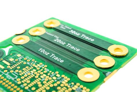
A thin layer of copper is then laminated onto the substrate using heat and pressure. The copper cladding can be applied on one or both sides of the substrate, depending on the PCB design requirements. The thickness of the copper layer is specified in ounces per square foot (oz/ft²), with common thicknesses ranging from 0.5 oz/ft² to 4 oz/ft².
Patterning and Etching
Once the copper cladding is in place, the desired circuit pattern is transferred onto the copper layer using a photolithographic process. A photoresist material is applied, exposed to light through a patterned mask, and developed to create a protective layer over the areas where copper should remain.
The exposed copper areas are then etched away using a chemical solution, typically ferric chloride or ammonium persulfate. This process removes the unwanted copper, leaving behind the desired circuit traces and pads.
Drilling and Plating
After etching, holes are drilled through the PCB to accommodate through-hole components and provide interconnections between layers in multi-layer boards. The drilled holes are then plated with copper to ensure electrical continuity and mechanical stability.
Solder Mask and Silkscreen
A solder mask layer is applied over the copper traces to protect them from oxidation and prevent solder bridging during assembly. The solder mask is typically a green or other colored polymer coating that leaves the pads and other designated areas exposed for soldering.
Finally, a silkscreen layer is added to the PCB, providing text, symbols, and markings for component placement and identification.

Advantages of Copper Based PCBs
Excellent Electrical Performance
Copper’s high electrical conductivity ensures excellent signal transmission and low resistance, resulting in superior electrical performance. This is particularly important for high-speed and high-frequency applications where signal integrity is critical.
Thermal Management
Copper’s thermal conductivity helps in dissipating heat generated by electronic components, preventing thermal damage and ensuring reliable operation. This is especially beneficial in high-power applications or densely populated PCBs where heat management is a key concern.
Cost-Effectiveness
Copper is relatively abundant and cost-effective compared to other conductive materials like gold or silver. Its widespread availability and lower cost make it an economically viable choice for mass production of PCBs.
Compatibility with Various Manufacturing Processes
Copper is compatible with a wide range of PCB manufacturing processes, including traditional subtractive methods and advanced additive techniques. This versatility allows for the fabrication of complex PCB designs with fine features and high precision.
Durability and Reliability
Copper based PCBs offer excellent durability and reliability. Copper’s mechanical strength and resistance to corrosion contribute to the long-term stability and performance of the PCB, even in harsh operating environments.

Applications of Copper Based PCBs
Consumer Electronics
Copper based PCBs are extensively used in consumer electronics, such as smartphones, tablets, laptops, televisions, and home appliances. The high electrical performance and cost-effectiveness of copper make it the preferred choice for these mass-produced devices.
Automotive Electronics
The automotive industry relies heavily on copper based PCBs for various electronic systems, including engine control units, infotainment systems, and advanced driver assistance systems (ADAS). Copper’s reliability and thermal management capabilities are crucial for the demanding operating conditions in automotive applications.
Industrial Automation and Control
Industrial automation and control systems employ copper based PCBs for their robustness and ability to withstand harsh industrial environments. Copper’s electrical and thermal properties ensure reliable operation in applications such as programmable logic controllers (PLCs), human-machine interfaces (HMIs), and industrial communication networks.
Medical Devices
Copper based PCBs are used in medical devices, including diagnostic equipment, patient monitoring systems, and implantable devices. Copper’s biocompatibility and ability to maintain signal integrity are essential for the precise and reliable functioning of these life-critical applications.
Aerospace and Defense
Aerospace and defense applications demand high-reliability PCBs that can withstand extreme conditions. Copper based PCBs are used in avionics, radar systems, satellites, and military communication equipment due to their robustness, thermal management capabilities, and ability to meet stringent performance requirements.
Copper PCB Design Considerations
Trace Width and Spacing
When designing copper based PCBs, it is important to consider the trace width and spacing. The trace width determines the current carrying capacity and resistance of the traces. Wider traces can handle higher currents and exhibit lower resistance. However, increasing trace width also increases the overall size of the PCB.
Trace spacing, on the other hand, affects signal integrity and crosstalk. Adequate spacing between traces is necessary to minimize electromagnetic interference and ensure proper signal isolation.
Via Design
Vias are conductive pathways that connect different layers of a multi-layer PCB. Proper via design is crucial for maintaining signal integrity and minimizing signal reflections. Via size, placement, and spacing should be carefully considered to ensure optimal electrical performance.
Impedance Control
Impedance control is essential for high-speed and high-frequency PCB designs. Copper trace width, thickness, and spacing play a significant role in determining the characteristic impedance of the traces. Proper impedance matching is necessary to minimize signal reflections and ensure reliable signal transmission.
Thermal Management
Effective thermal management is critical for the reliable operation of copper based PCBs. Proper copper thickness and distribution help in dissipating heat generated by electronic components. The use of thermal vias and copper pours can further enhance thermal performance by providing additional heat transfer paths.
Manufacturing Considerations
When designing copper based PCBs, it is important to consider the manufacturing capabilities and constraints of the PCB fabrication process. Factors such as minimum trace width, spacing, and hole size should be taken into account to ensure manufacturability and yield.
Collaborating closely with the PCB manufacturer and adhering to their design guidelines can help optimize the design for successful fabrication and assembly.
Frequently Asked Questions (FAQ)
1. What is the typical thickness of copper used in PCBs?
The thickness of copper used in PCBs is typically specified in ounces per square foot (oz/ft²). Common copper thicknesses range from 0.5 oz/ft² to 4 oz/ft², with 1 oz/ft² being the most widely used. The choice of copper thickness depends on the specific electrical and thermal requirements of the PCB design.
2. Can copper based PCBs be used for flexible applications?
Yes, copper based PCBs can be used for flexible applications. Flexible PCBs, also known as flex PCBs, utilize thin and flexible copper traces on a flexible substrate material such as polyimide. Flex PCBs offer improved mechanical flexibility and durability compared to rigid PCBs, making them suitable for applications that require bending or folding.
3. How does the copper thickness affect the current carrying capacity of PCB traces?
The current carrying capacity of PCB traces is directly proportional to the cross-sectional area of the copper trace. Increasing the copper thickness results in a larger cross-sectional area, allowing the trace to handle higher currents without excessive heating or voltage drop. The relationship between copper thickness and current carrying capacity is often specified in industry standards such as IPC-2221.
4. What is the role of solder mask on copper based PCBs?
The solder mask is a protective coating applied over the copper traces on a PCB. It serves several important functions:
- Insulation: The solder mask provides electrical insulation between adjacent traces, preventing short circuits and unintended connections.
- Protection: It protects the copper traces from oxidation, corrosion, and mechanical damage during handling and assembly.
- Solder Control: The solder mask defines the areas where solder should be applied during the assembly process, preventing solder bridging and ensuring proper component attachment.
5. How do copper based PCBs compare to aluminum based PCBs in terms of performance?
Copper based PCBs offer several advantages over aluminum based PCBs in terms of performance:
- Electrical Conductivity: Copper has a higher electrical conductivity compared to aluminum, resulting in lower resistance and better signal transmission.
- Thermal Conductivity: Copper also has superior thermal conductivity, allowing for more efficient heat dissipation and improved thermal management.
- Mechanical Strength: Copper provides better mechanical strength and durability compared to aluminum, making copper based PCBs more robust and reliable.
- Compatibility: Copper is compatible with a wider range of PCB manufacturing processes and assembly techniques, offering greater design flexibility.
While aluminum based PCBs have some niche applications where lightweight and cost are primary concerns, copper based PCBs remain the preferred choice for most electronic applications due to their superior performance and reliability.
Conclusion
Copper based PCBs have become the industry standard for modern electronics, offering excellent electrical and thermal properties, cost-effectiveness, and compatibility with various manufacturing processes. From consumer electronics to industrial automation, copper based PCBs find applications across a wide range of industries.
When designing copper based PCBs, careful consideration must be given to factors such as trace width and spacing, via design, impedance control, thermal management, and manufacturing constraints. By understanding these design considerations and collaborating with PCB manufacturers, engineers can create reliable and high-performance PCBs that meet the specific requirements of their applications.
As the demand for advanced electronic systems continues to grow, copper based PCBs will remain at the forefront of PCB technology, enabling the development of innovative and efficient electronic devices that shape our world.
Leave a Reply