Introduction to Buried Vias
In the world of electronic printed circuit boards (PCBs), a buried via is a specialized type of interconnect that plays a crucial role in the design and functionality of complex, multi-layer PCBs. This article will dive deep into the concept of buried vias, exploring their definition, applications, manufacturing processes, and the advantages they offer in modern PCB design.
What is a Via?
Before we delve into the specifics of buried vias, let’s first understand what a via is in the context of PCBs. A via, short for “vertical interconnect access,” is a small hole drilled through the layers of a PCB to establish an electrical connection between different layers. Vias are essential components in PCB design, allowing signals and power to be routed efficiently across the board.
Types of Vias
There are several types of vias used in PCB design, each serving a specific purpose:
| Via Type | Description |
|---|---|
| Through Hole Via | A via that goes through all layers of the PCB, from top to bottom. |
| Blind Via | A via that connects an outer layer to an inner layer, but does not go through the entire board. |
| Buried Via | A via that connects two or more inner layers, without reaching the outer layers. |
| Microvia | A small via, typically less than 0.15mm in diameter, used for high-density interconnects. |
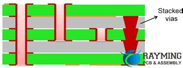
What is a Buried Via?
A buried via is a type of via that is used to establish electrical connections between two or more inner layers of a multi-layer PCB, without extending to the outer layers of the board. Unlike through hole vias, which are visible on both the top and bottom surfaces of the PCB, buried vias are completely hidden within the inner layers of the board.
How Buried Vias are Manufactured
The manufacturing process for buried vias involves several steps:
-
Layer Preparation: The inner layers of the PCB are patterned and etched with the necessary circuit traces and pad locations for the buried vias.
-
Via Drilling: Holes are drilled through the specific inner layers that need to be connected by the buried vias. These holes do not extend to the outer layers of the board.
-
Via Plating: The drilled holes are plated with a conductive material, typically copper, to establish electrical connectivity between the connected layers.
-
Lamination: The inner layers, along with the buried vias, are laminated together with the other layers of the PCB using heat and pressure.
-
Outer Layer Processing: The outer layers of the PCB are then patterned, etched, and finished as required, while the buried vias remain hidden within the inner layers.
Advantages of Buried Vias
Buried vias offer several advantages in PCB design:
-
Space Savings: By utilizing the inner layers of the PCB for interconnects, buried vias help to save space on the outer layers, allowing for more compact and efficient board layouts.
-
Signal Integrity: Buried vias can provide shorter and more direct signal paths between layers, reducing signal loss and improving overall signal integrity.
-
Reduced EMI: By keeping the vias within the inner layers, buried vias can help to reduce electromagnetic interference (EMI) that may otherwise be caused by exposed vias on the outer layers.
-
Design Flexibility: Buried vias allow for greater flexibility in PCB design, enabling more complex routing and layer stacking arrangements.

Applications of Buried Vias
Buried vias find applications in various industries and products where PCB design complexity and performance are critical factors:
High-Density Interconnect (HDI) PCBs
HDI PCBs are characterized by their high component density and fine-pitch traces. Buried vias are extensively used in HDI designs to achieve the required interconnect density and signal integrity. By using buried vias, designers can route signals between layers without consuming valuable real estate on the outer layers.
Multilayer PCBs
As the number of layers in a PCB increases, the use of buried vias becomes increasingly important. Multilayer PCBs, often used in advanced electronic devices, rely on buried vias to establish reliable interconnects between the inner layers. This allows for efficient routing of signals and power across the board, while minimizing the overall thickness of the PCB.
High-Speed Digital Designs
In high-speed digital circuits, such as those found in modern communication systems and computing devices, signal integrity is of utmost importance. Buried vias play a crucial role in maintaining signal quality by providing short, direct paths between layers. By reducing the signal path length and minimizing the number of vias a signal must traverse, buried vias help to reduce signal reflections, crosstalk, and other signal integrity issues.
RF and Microwave PCBs
Radio frequency (RF) and microwave PCBs often employ buried vias to optimize signal propagation and minimize losses. In these high-frequency applications, the placement and design of vias are critical to maintaining the desired impedance and reducing unwanted signal coupling. Buried vias allow designers to carefully control the via geometry and spacing, ensuring optimal performance in RF and microwave circuits.

Design Considerations for Buried Vias
When incorporating buried vias into a PCB design, there are several key considerations to keep in mind:
Via Size and Spacing
The size and spacing of buried vias should be carefully chosen based on the specific requirements of the design. Smaller via sizes allow for higher interconnect density but may pose manufacturing challenges. Adequate spacing between vias is necessary to ensure reliable plating and to minimize signal coupling.
Layer Stackup
The layer stackup of the PCB should be designed with buried vias in mind. The placement of buried vias within the stackup can impact signal integrity, power distribution, and overall board thickness. Designers should work closely with the PCB fabricator to determine the optimal layer stackup for their specific application.
Via Positioning
The positioning of buried vias should be carefully considered to minimize signal path lengths and to avoid any potential signal integrity issues. Vias should be placed as close as possible to the components they are connecting to reduce parasitic effects and to improve signal quality.
Manufacturing Constraints
Buried vias introduce additional complexity to the PCB manufacturing process, and designers must be aware of the capabilities and limitations of their chosen fabricator. Factors such as via size, aspect ratio, and plating requirements should be discussed with the fabricator to ensure manufacturability and reliability.

Frequently Asked Questions (FAQ)
-
Q: What is the difference between a buried via and a blind via?
A: A buried via connects two or more inner layers of a PCB without reaching the outer layers, while a blind via connects an outer layer to an inner layer but does not go through the entire board. -
Q: Can buried vias be used in single-layer PCBs?
A: No, buried vias are only applicable in multi-layer PCBs, as they are used to connect inner layers without reaching the outer layers. -
Q: Are buried vias more expensive than through hole vias?
A: Yes, buried vias generally add to the manufacturing cost of a PCB due to the additional processing steps involved, such as multiple drilling and plating operations. -
Q: Can buried vias improve signal integrity in high-speed designs?
A: Yes, buried vias can help improve signal integrity by providing shorter, more direct signal paths between layers, reducing signal reflections and crosstalk. -
Q: Are there any limitations on the size and aspect ratio of buried vias?
A: Yes, the size and aspect ratio of buried vias are typically limited by the capabilities of the PCB fabricator. Designers should consult with their fabricator to determine the achievable via dimensions for their specific design.
Conclusion
Buried vias are a critical component in modern PCB design, enabling the creation of complex, high-performance electronic devices. By providing efficient and reliable interconnects between inner layers, buried vias offer numerous advantages, including space savings, improved signal integrity, and greater design flexibility.
As PCB designs continue to push the boundaries of complexity and performance, the use of buried vias will remain essential in achieving the required interconnect density and signal quality. Designers must carefully consider the placement, size, and spacing of buried vias, as well as the manufacturing constraints, to ensure optimal functionality and reliability of their PCB designs.
By understanding the principles and applications of buried vias, PCB designers can harness their potential to create innovative and high-performance electronic products across a wide range of industries.
Leave a Reply