What is Through-Hole Technology?
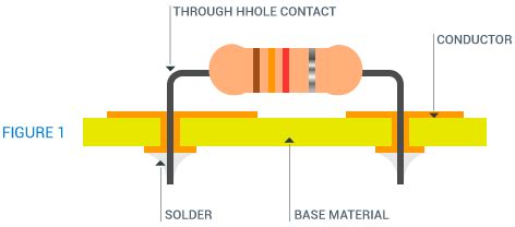
Through-hole technology, also known as through-hole mounting (THM) or plated-through-hole (PTH), is a method of mounting electronic components on printed circuit boards (PCBs). In this process, component leads are inserted through drilled holes in the PCB and soldered to pads on the opposite side, creating a strong mechanical and electrical connection.
Advantages of Through-Hole Assembly
- Durability: Through-hole components are known for their robustness and ability to withstand mechanical stress and vibration.
- Reliability: The strong solder joint created in through-hole assembly ensures a reliable electrical connection.
- Easy to replace: Through-hole components can be easily replaced or repaired using manual soldering techniques.
- Suitable for high-power applications: Through-hole components can handle higher power ratings compared to surface-mount devices (SMDs).
Disadvantages of Through-Hole Assembly
- Larger footprint: Through-hole components occupy more space on a PCB compared to SMDs, limiting the component density.
- Higher assembly costs: Through-hole assembly is generally more time-consuming and labor-intensive than surface-mount assembly, resulting in higher manufacturing costs.
- Limited PCB design flexibility: The need for drilled holes in through-hole assembly restricts the routing of traces on the PCB, reducing design flexibility.
Through-Hole Assembly Process
The through-hole assembly process involves several steps, as outlined below:
1. PCB Fabrication
The first step in through-hole assembly is the fabrication of the printed circuit board. This process includes:
- Designing the PCB layout using electronic design automation (EDA) software
- Generating Gerber files for manufacturing
- Fabricating the PCB substrate, which involves applying copper layers, etching traces, and drilling holes
2. Component Insertion
Once the PCB is fabricated, the next step is to insert the through-hole components into the designated holes. This can be done manually or using automated insertion machines.
- Manual insertion: For small-scale production or prototypes, components are inserted by hand using pliers or tweezers.
- Automated insertion: In high-volume manufacturing, machines like axial or radial insertion machines are used to automatically insert components into the PCB.
3. Soldering
After component insertion, the PCB undergoes soldering to create a permanent electrical and mechanical connection between the component leads and the PCB pads.
- Wave soldering: The most common method for through-hole soldering is wave soldering. In this process, the PCB is passed over a molten solder wave, which wets the component leads and PCB pads, creating a solder joint.
- Hand soldering: For small batches or repairs, manual soldering using a soldering iron is employed.
4. Inspection and Testing
Following the soldering process, the assembled PCBs are inspected and tested to ensure the quality and functionality of the final product.
- Visual inspection: Assembled PCBs are visually inspected for any soldering defects, such as bridging, insufficient solder, or cold solder joints.
- Automated optical inspection (AOI): AOI machines use cameras and image processing algorithms to detect soldering defects and component placement issues.
- Electrical testing: The assembled PCBs undergo electrical testing to verify their functionality and performance. This may include in-circuit testing (ICT), functional testing, or boundary scan testing.
5. Rework and Repair
If any defects are found during the inspection and testing phase, the PCBs are sent for rework and repair.
- Desoldering: Faulty components are desoldered using desoldering tools like desoldering pumps, desoldering wicks, or desoldering stations.
- Component replacement: Once the faulty component is removed, a new component is inserted and soldered in its place.
- Re-inspection: After rework, the PCB is inspected and tested again to ensure that the issue has been resolved.

Through-Hole Components
Through-hole components come in various packages and form factors. Some common through-hole component packages include:
- Axial lead: Components with leads extending from opposite ends of the component body, such as resistors, capacitors, and diodes.
- Radial lead: Components with leads extending from the same side of the component body, such as electrolytic capacitors and LED lamps.
- DIP (Dual Inline Package): Integrated circuits with two parallel rows of leads, such as DIP ICs and sockets.
- SIP (Single Inline Package): Components with a single row of leads, such as resistor networks and connectors.
| Component Package | Description | Examples |
|---|---|---|
| Axial Lead | Leads extend from opposite ends of the component body | Resistors, capacitors, diodes |
| Radial Lead | Leads extend from the same side of the component body | Electrolytic capacitors, LED lamps |
| DIP | Integrated circuits with two parallel rows of leads | DIP ICs, sockets |
| SIP | Components with a single row of leads | Resistor networks, connectors |

Design Considerations for Through-Hole Assembly
When designing a PCB for through-hole assembly, several factors need to be considered:
1. Hole Size and Pad Diameter
The hole size and pad diameter should be appropriate for the component lead size to ensure a proper fit and reliable soldering. The hole size is typically 0.1 mm to 0.2 mm larger than the lead diameter, while the pad diameter is usually 2 to 3 times the hole size.
2. Component Spacing
Adequate spacing between components is essential to facilitate soldering and avoid potential short circuits. The minimum spacing depends on factors such as the component package, lead size, and soldering method employed.
3. Component Orientation
Component orientation should be clearly indicated on the PCB layout to ensure correct placement during assembly. This can be done using silkscreen markings or assembly drawings.
4. Thermal Management
Through-hole components that generate significant heat, such as power transistors or voltage regulators, may require additional thermal management. This can be achieved by using thermal relief pads, heat sinks, or thermal vias to dissipate heat effectively.

Comparison with Surface-Mount Technology (SMT)
While through-hole technology has been widely used for decades, surface-mount technology (SMT) has gained popularity in recent years due to its advantages in miniaturization and high-volume production.
| Aspect | Through-Hole Technology | Surface-Mount Technology |
|---|---|---|
| Component size | Larger, limited miniaturization | Smaller, enables higher component density |
| PCB real estate | Requires more space due to drilled holes | Components mounted directly on PCB surface, saving space |
| Assembly process | Manual or automated insertion, wave or hand soldering | Automated pick-and-place machines, reflow soldering |
| Manufacturing cost | Higher assembly cost due to manual labor | Lower assembly cost due to automation |
| Durability | More robust, suitable for high-stress environments | Less durable, may be affected by vibration and thermal stress |
| Rework and repair | Easier to replace or repair individual components | More challenging to rework or repair individual components |
| High-frequency performance | Longer leads may introduce parasitic inductance | Shorter connections, better high-frequency performance |
Despite the advantages of SMT, through-hole technology remains relevant in certain applications, such as:
- High-power electronics: Through-hole components can handle higher power ratings and better thermal dissipation.
- Prototyping and low-volume production: Through-hole assembly is often more cost-effective for small-scale production or prototyping.
- Mechanical stress: Through-hole components are more resistant to mechanical stress and vibration, making them suitable for high-reliability applications.
Frequently Asked Questions (FAQ)
1. What is the difference between through-hole and surface-mount technology?
Through-hole technology involves inserting component leads through drilled holes in the PCB and soldering them to pads on the opposite side. Surface-mount technology (SMT) involves placing components directly onto pads on the PCB surface and soldering them using reflow soldering.
2. Can through-hole and surface-mount components be used on the same PCB?
Yes, it is possible to use both through-hole and surface-mount components on the same PCB. This is called a mixed-technology or hybrid assembly. However, the assembly process becomes more complex as it involves both through-hole and SMT assembly steps.
3. Are through-hole components becoming obsolete?
While surface-mount technology has become more prevalent in recent years, through-hole components are still widely used in certain applications, such as high-power electronics, automotive systems, and military equipment. Through-hole technology is also valuable for prototyping and low-volume production.
4. What is the most common soldering method for through-hole assembly?
Wave soldering is the most common soldering method for through-hole assembly in high-volume production. In this process, the PCB is passed over a molten solder wave, which wets the component leads and PCB pads, creating a solder joint.
5. Can through-hole components be replaced with surface-mount equivalents?
In many cases, through-hole components can be replaced with surface-mount equivalents. However, it is essential to consider factors such as power rating, thermal dissipation, and mechanical stress when making the switch. Some applications may still require through-hole components for optimal performance and reliability.
Leave a Reply