Introduction to PCB Fabrication
Printed Circuit Board (PCB) fabrication is a complex process that involves several steps to create a functional and reliable board. PCBs are essential components in modern electronic devices, ranging from smartphones and computers to industrial equipment and aerospace systems. The PCB fabrication process has evolved over the years, incorporating advanced technologies and techniques to meet the growing demands for smaller, faster, and more efficient electronic devices.
In this article, we will explore the various steps involved in the PCB fabrication process, focusing on the manufacturing techniques used to create high-quality PCBs. We will also discuss the importance of each step and how they contribute to the overall performance and reliability of the final product.
Step 1: PCB Design and Layout
1.1 Schematic Design
The first step in the PCB fabrication process is the design and layout of the circuit. This begins with creating a schematic diagram that represents the electrical connections and components of the circuit. The schematic is created using specialized Electronic Design Automation (EDA) software, such as Altium Designer, Eagle, or KiCad.
The schematic design involves the following tasks:
- Selecting the appropriate components for the circuit
- Defining the electrical connections between components
- Assigning component values and tolerances
- Checking the schematic for errors and inconsistencies
1.2 PCB Layout
Once the schematic design is complete, the next step is to create the PCB layout. The layout determines the physical arrangement of components and traces on the board. The PCB layout is created using the same EDA software used for schematic design.
The PCB layout process involves the following tasks:
- Placing components on the board
- Routing traces between components
- Defining the board outline and mounting holes
- Adding text and graphics for assembly and identification
- Checking the layout for design rule violations and manufacturability
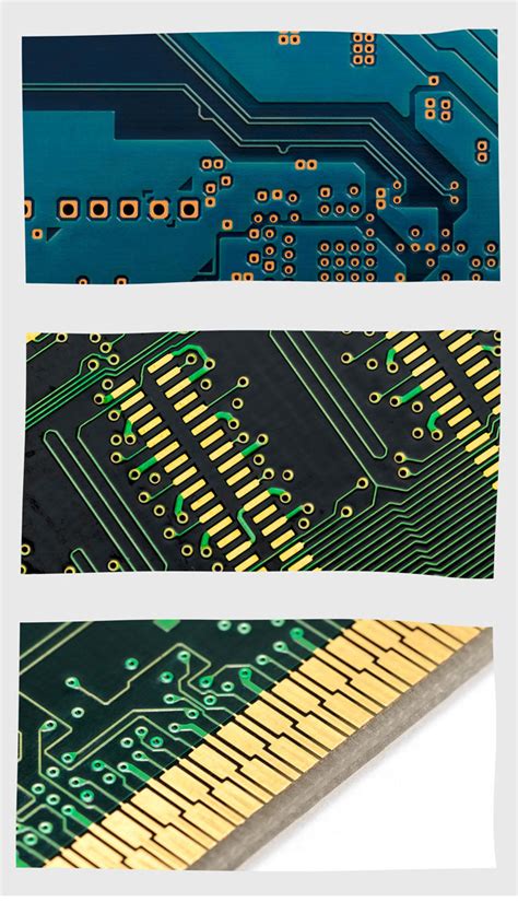
The PCB layout is a critical step in the fabrication process, as it directly affects the performance, reliability, and manufacturability of the final product. A well-designed layout ensures proper signal integrity, minimizes electromagnetic interference (EMI), and facilitates efficient manufacturing.

Step 2: PCB Fabrication
2.1 Material Selection
The choice of PCB material depends on the specific requirements of the application, such as electrical properties, thermal stability, and mechanical strength. The most common PCB materials are:
- FR-4: A glass-reinforced epoxy laminate, widely used for general-purpose applications
- High-Tg FR-4: An enhanced version of FR-4 with improved thermal stability
- Polyimide: A high-performance material with excellent thermal and mechanical properties
- PTFE: A low-loss material for high-frequency applications
- Aluminum: A metal-core material for high-power and heat-dissipation applications
2.2 Copper Clad Laminate
The PCB fabrication process begins with a copper-clad laminate, which consists of a thin layer of copper foil bonded to one or both sides of the insulating substrate material. The thickness of the copper foil ranges from 0.5 oz to 4 oz per square foot, with 1 oz being the most common.
2.3 Drilling
The next step is to drill holes in the laminate for through-hole components and vias. The drilling process is performed using high-speed CNC drilling machines equipped with carbide or diamond-tipped drill bits. The drill bit size and location are determined by the PCB layout data.
2.4 Plating
After drilling, the holes are plated with a thin layer of copper to provide electrical connectivity between the layers. The plating process involves the following steps:
- Desmear: Removing the resin smear from the drilled holes to ensure proper copper adhesion
- Electroless Copper Deposition: Depositing a thin layer of copper on the hole walls using a chemical process
- Electrolytic Copper Plating: Building up the copper thickness in the holes and on the surface using an electric current
2.5 Patterning
The next step is to create the copper pattern on the board according to the PCB layout. This is done using a photolithographic process, which involves the following steps:
- Applying a photoresist layer on the copper surface
- Exposing the photoresist to UV light through a photomask that contains the copper pattern
- Developing the photoresist to remove the unexposed areas
- Etching away the unwanted copper using a chemical etchant
- Stripping the remaining photoresist
2.6 Soldermask Application
A soldermask is a protective layer applied over the copper pattern to prevent oxidation and provide insulation between the copper traces. The soldermask is typically green, but other colors are also available. The soldermask application process involves the following steps:
- Applying the soldermask ink on the board
- Exposing the soldermask to UV light through a photomask that defines the openings for pads and vias
- Developing the soldermask to remove the unexposed areas
- Curing the soldermask to ensure proper adhesion and durability
2.7 Silkscreen
The final step in the PCB fabrication process is to apply the silkscreen, which is a layer of text and graphics used for component identification and assembly instructions. The silkscreen is typically white, but other colors are also available. The silkscreen application process is similar to the soldermask application, using a photolithographic process.

Step 3: PCB Assembly
3.1 Surface Mount Technology (SMT)
Surface Mount Technology (SMT) is a method of assembling electronic components directly onto the surface of a PCB. SMT components are smaller and have leads that are soldered directly to pads on the board surface. The SMT assembly process involves the following steps:
- Solder Paste Application: Applying a thin layer of solder paste on the component pads using a stencil or screen printing process
- Component Placement: Placing the SMT components on the solder paste using a pick-and-place machine
- Reflow Soldering: Passing the board through a reflow oven to melt the solder paste and form a permanent connection between the components and the board
3.2 Through-Hole Technology (THT)
Through-Hole Technology (THT) is a method of assembling electronic components with leads that are inserted into holes drilled in the PCB and soldered to pads on the opposite side of the board. THT components are larger and more robust than SMT components. The THT assembly process involves the following steps:
- Component Insertion: Inserting the THT component leads into the drilled holes in the board
- Wave Soldering: Passing the board over a molten solder wave to form a permanent connection between the component leads and the board
3.3 Mixed Technology
Many PCBs use a combination of SMT and THT components, known as mixed technology. In this case, the SMT components are assembled first, followed by the THT components. The board then goes through both reflow and wave soldering processes to ensure proper connection of all components.

Step 4: PCB Testing and Inspection
4.1 Visual Inspection
After the PCB assembly process, the board undergoes visual inspection to check for any obvious defects or missing components. This is typically done using automated optical inspection (AOI) machines, which use cameras and image processing software to compare the assembled board to the original PCB layout data.
4.2 Electrical Testing
The next step is to perform electrical testing to ensure that the board functions as intended. This involves using specialized test equipment to verify the following:
- Continuity: Checking for proper electrical connection between components and traces
- Isolation: Checking for unwanted shorts or leakage between traces
- Functionality: Verifying that the board performs the desired functions
Electrical testing can be done using various methods, such as:
- In-Circuit Testing (ICT): Testing individual components and nets using a bed-of-nails fixture
- Flying Probe Testing: Testing specific points on the board using movable probes
- Functional Testing: Testing the overall functionality of the board using a custom test fixture or software
4.3 Environmental Testing
Depending on the application and requirements, the PCB may also undergo environmental testing to ensure its reliability and durability under various conditions. This may include:
- Temperature Cycling: Exposing the board to alternating high and low temperatures to check for thermal stress and expansion
- Humidity Testing: Exposing the board to high humidity levels to check for moisture resistance
- Vibration Testing: Subjecting the board to mechanical vibrations to check for structural integrity
- Burn-In Testing: Operating the board at elevated temperatures for an extended period to check for early failures
Step 5: PCB Finishing and Packaging
5.1 Surface Finishing
To enhance the solderability and protection of the exposed copper pads and vias, a surface finish is applied to the PCB. The most common surface finishes are:
- Hot Air Solder Leveling (HASL): Dipping the board in molten solder and using hot air to level the surface
- Electroless Nickel Immersion Gold (ENIG): Plating the copper with a layer of nickel followed by a thin layer of gold
- Immersion Silver (IAg): Plating the copper with a thin layer of silver
- Immersion Tin (ISn): Plating the copper with a thin layer of tin
- Organic Solderability Preservative (OSP): Applying an organic coating to the copper to prevent oxidation
5.2 Packaging and Shipping
After the surface finishing process, the PCBs are packaged and shipped to the customer. The packaging method depends on the size, quantity, and fragility of the boards. Common packaging methods include:
- Vacuum packaging: Sealing the boards in a vacuum bag to prevent moisture and contamination
- ESD packaging: Using anti-static bags and materials to protect the boards from electrostatic discharge
- Bulk packaging: Packing multiple boards in a single box or container for large quantities
- Individual packaging: Packing each board separately in its own bag or box for small quantities or high-value boards
Frequently Asked Questions (FAQ)
- What is the difference between SMT and THT assembly?
-
SMT (Surface Mount Technology) involves assembling components directly onto the surface of the PCB, while THT (Through-Hole Technology) involves inserting component leads into holes drilled in the board and soldering them to pads on the opposite side. SMT components are smaller and more suitable for high-density designs, while THT components are larger and more robust.
-
What is the purpose of the soldermask layer on a PCB?
-
The soldermask is a protective layer applied over the copper pattern to prevent oxidation and provide insulation between the copper traces. It also helps to prevent solder bridging and short circuits during the assembly process.
-
Why is electrical testing important in PCB fabrication?
-
Electrical testing is crucial to ensure that the PCB functions as intended and meets the required specifications. It helps to identify any defects or issues related to continuity, isolation, and functionality, which can affect the performance and reliability of the final product.
-
What are the advantages of using ENIG surface finish on a PCB?
-
ENIG (Electroless Nickel Immersion Gold) provides excellent solderability, corrosion resistance, and shelf life compared to other surface finishes. The nickel layer provides a barrier against copper diffusion, while the gold layer prevents oxidation and ensures good wettability for soldering.
-
How can I ensure the quality and reliability of my PCBs during the fabrication process?
- To ensure the quality and reliability of your PCBs, it is important to work with a reputable PCB manufacturer that follows industry standards and best practices. This includes using high-quality materials, adhering to strict process controls, and performing thorough testing and inspection at every stage of the fabrication process. It is also important to provide clear and accurate design files and specifications to minimize the risk of errors and delays.
Conclusion
The PCB fabrication process is a complex and multi-step process that requires precision, expertise, and attention to detail. From the initial design and layout to the final packaging and shipping, each step plays a critical role in ensuring the quality, reliability, and functionality of the final product.
By understanding the various steps and techniques involved in PCB fabrication, designers and engineers can make informed decisions and optimize their designs for manufacturability and performance. Working closely with a reputable PCB manufacturer and following industry best practices can help to minimize risks, reduce costs, and ensure a successful outcome.
As technology continues to evolve and the demand for smaller, faster, and more complex electronic devices grows, the PCB fabrication process will continue to adapt and innovate to meet these challenges. By staying up-to-date with the latest advancements and techniques, designers and manufacturers can stay ahead of the curve and deliver high-quality PCBs that meet the needs of today’s and tomorrow’s electronic devices.
| Step | Process | Description |
|---|---|---|
| 1 | PCB Design and Layout | Creating the schematic and PCB layout using EDA software |
| 2 | PCB Fabrication | Manufacturing the PCB using various techniques and materials |
| 3 | PCB Assembly | Assembling the components onto the PCB using SMT, THT, or mixed technology |
| 4 | PCB Testing and Inspection | Verifying the quality and functionality of the assembled PCB |
| 5 | PCB Finishing and Packaging | Applying surface finish and packaging the PCBs for shipping |
Leave a Reply