Introduction to RF PCBs
Radio frequency (RF) printed circuit boards (PCBs) are designed to operate at high frequencies from 3 kHz to 300 GHz. They are used in various wireless communication devices like cell phones, WiFi routers, radars, satellites etc. The design and material requirements of RF PCBs differ considerably from traditional PCBs due to the high frequencies involved.
Key Design Considerations
Several factors have to be considered when designing RF PCBs:
- Impedance control – Maintaining 50-ohm controlled impedance is critical for minimizing signal loss and reflections. This requires careful PCB stackup design.
- Signal integrity – RF signals can be affected by crosstalk and noise. Careful routing and grounding techniques should be used.
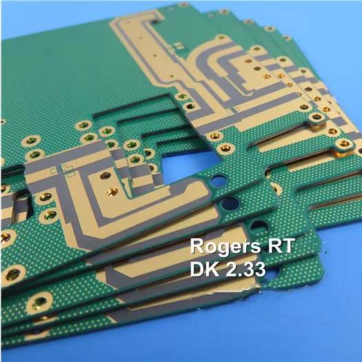
- Materials – FR-4 is not suitable for RF PCBs. High frequency laminates like Rogers and Taconic with lower loss are used.
- Shielding – Sensitive traces should be shielded to prevent interference and leakage.
- Connectors – High frequency connectors like SMA, SSMT are used. Transitions to these should be impedance matched.
Typical RF PCB Materials
| Material | Dielectric Constant | Loss Tangent | Frequency Range |
|---|---|---|---|
| Rogers RO4003C | 3.38 | 0.0027 | Up to 10 GHz |
| Rogers RO4350B | 3.48 | 0.0037 | Up to 20 GHz |
| Taconic RF-35 | 3.5 | 0.0018 | Up to 30 GHz |
RF PCB Applications
Some common applications of RF PCBs include:
Cellular Communications
RF PCBs are extensively used in cell phones, base stations, towers and other cellular network equipment. Frequencies up to 5G spectrum (6 GHz) need to be handled.
Wireless Local Area Networks
WiFi routers and access points use RF PCBs operating at 2.4 GHz and 5 GHz bands. High speed data transfer is enabled through technologies like 802.11ac.
Satellite Communications
Satellite payloads have RF circuitry operating at microwave frequencies up to 30 GHz and beyond. High frequency laminates like Taconic RF-35 are suitable for space applications.
Radio and Radar Systems
Military radar and software-defined radio systems use RF PCBs for transmit/receive modules and antenna beamformers working up to Ku band.
Challenges in RF PCB Design

Some key challenges faced during RF PCB design are:
- Achieving impedance matching and minimizing reflections. Careful stackup design and stub tuning is required.
- Preventing electromagnetic interference through proper grounding, shielding and isolation.
- Maintaining signal integrity through controlled routing and layer transitions.
- Selecting suitable materials based on frequency range and loss requirements.
- Testing RF performance like insertion loss, return loss, gain etc. Complex test setups may be needed.
- Thermal management due to high power density at RF frequencies.
Frequently Asked Questions
What are some common RF connectors used on PCBs?
Some common RF connectors are SMA, SSMT, 2.92mm, 2.4mm, 1.85mm and 1.0mm. The size typically decreases with increasing frequency. Care must be taken to properly match the impedance at the transition from PCB trace to connector.
How is shielding implemented on RF PCBs?
Sensitive traces are shielded using techniques like grounded copper pours, metal enclosures/cans around critical areas of the PCB, placement of ground vias around traces. EM simulation helps to design effective shielding.
What are thermal challenges in RF PCBs?
High frequency signals can cause localized heating of PCBs. Thermal vias, large copper planes and metal core PCBs help conduct heat efficiently. Fans may be used in very high power designs. Proper thermal management is critical for reliability.
How are RF PCBs tested during fabrication?
Testing includes S-parameter measurements like insertion loss, return loss, gain, phase response using Vector Network Analyzers. Time domain reflectometry is used to test impedance variations. Near-field scanning can detect EMI issues.
What fabrication tolerances are required for RF PCBs?
Much tighter fabrication tolerances are needed for RF PCBs compared to digital PCBs. Trace width and dielectric thickness should be controlled to +/- 0.05mm or better for consistent impedance. Registration accuracy better than 0.1mm helps avoid signal integrity issues.
Leave a Reply