RF PCB Layout
High frequency printed circuit board (PCB) layout requires special design considerations to ensure signal integrity and prevent electromagnetic interference (EMI). Here are some key guidelines for rf PCB layout:
Impedance Control
- Match impedance of traces to components to prevent signal reflection and losses. Common impedance values are 50Ω and 75Ω.
- Use impedance matching techniques like width tuning, adding gaps between ground planes and traces.
- Minimize abrupt changes in trace width that cause impedance discontinuities.
Bypassing and Decoupling
- Place bypass/decoupling capacitors as close as possible to IC power pins.
- Use multiple capacitors for high frequency decoupling (e.g. 0.1μF, 1μF).
- Avoid vias in decoupling capacitor ground loops.
Grounding
- Use large area ground planes to provide low impedance return paths.
- Connect ground planes with multiple vias placed closely.
- Isolate digital and analog grounds to prevent noise coupling.
Signal Routing
- Route critical signals first using controlled impedance lines.
- Avoid 90° turns. Use 45° angled traces or arc traces instead.
- Keep out zones around connectors to avoid accidental traces shorting pins.
Shielding
- Enclose RF circuitry in shielded compartments to contain EMI.
- Use electromagnetic bandgaps in board layout to isolate circuits.
- Place sensitive circuits away from noisy components.
Component Placement
- Place active components first, then passive components.
- Group associated components together.
- Ensure components match line impedance to minimize reflections.
Stackup Design
- Use at least 4 layer board – signal, ground, power, signal.
- Place ground plane close to outer layers where RF signals route.
- Use thicker dielectric materials to reduce losses.
Testability
- Include test points, vias and pads for RF connectors and cables.
- Allow access to tuning components like capacitors and inductors.
- Follow design rules for PCB fabrication and assembly.
Common RF Layout Challenges
| Challenge | Mitigation Techniques |
|---|---|
| Impedance Discontinuities | Gradual width transitions, back drilling vias |
| EMI and Crosstalk | Ground planes, shielding, bandgaps |
| Signal Losses | Impedance control, vias, materials |
| Radiation | Shielding, wire bonds, absorbers |
| Thermal Issues | Thermal vias, copper balancing, heatsinks |
Frequently Asked Questions

What are some key considerations for controlled impedance traces?
Some key factors are: trace width, dielectric thickness, dielectric constant, presence of a ground plane, distance to ground plane. These parameters determine the characteristic impedance based on equations like the stripline or microstrip models.
Why is decoupling important for RF circuits?
Decoupling capacitors provide charge reservoirs near active devices to handle transient current demands. Without proper decoupling, voltage drops can occur during state changes, causing noise or functional issues.
What techniques can reduce EMI in a PCB design?
Shielding sensitive traces, routing signals orthogonally, using ground planes, bandgap structures, and differential signaling pairs all help contain electromagnetic radiation and reduce EMI. Proper component placement also prevents emissions from aggregating.
How can thermal issues be addressed in RF PCBs?
Strategic use of thermal vias under hot components spreads heat into ground planes. Copper balancing helps avoid hotspots. Heatsinks or active cooling may be required for high power circuits. Thermal modeling early in design helps identify problems.
What are common stackup arrangements for RF designs?
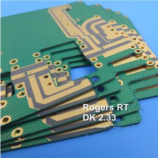
Four layer designs with a full ground plane near the RF layer are typical. High frequency boards may need thicker dielectrics like RF-35 or RF-43 to reduce losses. More layers can be used for complex designs, with care taken in layer ordering.
Leave a Reply