Introduction to PCB Stackup
A PCB stackup refers to the arrangement of copper and insulating layers that make up a printed circuit board (PCB). It is a critical aspect of PCB design as it determines the board’s electrical properties, mechanical strength, and manufacturability. In this article, we will dive into the standard stackup for multilayer PCBs provided by RAYPCB, a leading PCB manufacturer.
Why is PCB Stackup Important?
PCB stackup plays a crucial role in the performance and reliability of electronic devices. Here are some reasons why PCB stackup is important:
-
Signal Integrity: The arrangement of layers in a PCB stackup can significantly impact the signal integrity. Proper stackup design helps minimize crosstalk, electromagnetic interference (EMI), and signal reflections, ensuring reliable signal transmission.
-
Impedance Control: PCB stackup influences the characteristic impedance of transmission lines. By carefully selecting the dielectric materials and thicknesses, designers can achieve the desired impedance for high-speed signals, preventing signal distortion and reflections.
-
Power Distribution: The placement of power and ground planes in the stackup affects the power distribution network’s effectiveness. A well-designed stackup ensures a low-impedance path for power delivery, minimizing voltage drops and reducing electromagnetic emissions.
-
Mechanical Strength: The number and arrangement of layers in a PCB stackup contribute to the board’s mechanical strength. Proper stackup design helps prevent warping, twisting, and other mechanical issues that can arise during manufacturing and assembly.
-
Manufacturing Feasibility: The choice of stackup directly impacts the manufacturing process. It determines the number of lamination cycles, drilling requirements, and the overall complexity of the PCB fabrication. A well-planned stackup ensures manufacturability and reduces the risk of production issues.
RAYPCB Standard Stackup for Multilayer PCBs
RAYPCB offers a standard stackup for multilayer PCBs that has been optimized for signal integrity, power distribution, and manufacturability. Let’s explore the details of this stackup.
4-Layer PCB Stackup
For 4-layer PCBs, RAYPCB recommends the following stackup:
| Layer | Material | Thickness (mm) |
|---|---|---|
| Top Copper | Copper | 0.035 |
| Dielectric 1 | FR-4 | 0.2 |
| Inner Layer 1 | Copper | 0.035 |
| Dielectric 2 | FR-4 | 0.7 |
| Inner Layer 2 | Copper | 0.035 |
| Dielectric 3 | FR-4 | 0.2 |
| Bottom Copper | Copper | 0.035 |
In this stackup, the top and bottom layers are used for signal routing, while the inner layers are dedicated to power and ground planes. The dielectric material used is FR-4, a common choice for PCBs due to its good electrical and mechanical properties.
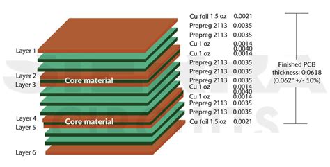
6-Layer PCB Stackup
For 6-layer PCBs, RAYPCB suggests the following stackup:
| Layer | Material | Thickness (mm) |
|---|---|---|
| Top Copper | Copper | 0.035 |
| Dielectric 1 | FR-4 | 0.2 |
| Inner Layer 1 | Copper | 0.035 |
| Dielectric 2 | FR-4 | 0.2 |
| Inner Layer 2 | Copper | 0.035 |
| Dielectric 3 | FR-4 | 0.7 |
| Inner Layer 3 | Copper | 0.035 |
| Dielectric 4 | FR-4 | 0.2 |
| Inner Layer 4 | Copper | 0.035 |
| Dielectric 5 | FR-4 | 0.2 |
| Bottom Copper | Copper | 0.035 |
In this 6-layer stackup, the top and bottom layers are used for signal routing, while the inner layers are allocated for power, ground, and additional signal layers. The dielectric thicknesses are chosen to maintain a consistent impedance throughout the board.
8-Layer PCB Stackup
For more complex designs requiring 8 layers, RAYPCB provides the following standard stackup:
| Layer | Material | Thickness (mm) |
|---|---|---|
| Top Copper | Copper | 0.035 |
| Dielectric 1 | FR-4 | 0.2 |
| Inner Layer 1 | Copper | 0.035 |
| Dielectric 2 | FR-4 | 0.2 |
| Inner Layer 2 | Copper | 0.035 |
| Dielectric 3 | FR-4 | 0.2 |
| Inner Layer 3 | Copper | 0.035 |
| Dielectric 4 | FR-4 | 0.7 |
| Inner Layer 4 | Copper | 0.035 |
| Dielectric 5 | FR-4 | 0.2 |
| Inner Layer 5 | Copper | 0.035 |
| Dielectric 6 | FR-4 | 0.2 |
| Inner Layer 6 | Copper | 0.035 |
| Dielectric 7 | FR-4 | 0.2 |
| Bottom Copper | Copper | 0.035 |
This 8-layer stackup provides ample space for signal routing, power distribution, and ground planes. The symmetrical arrangement of layers helps minimize warping and ensures a balanced construction.

Benefits of RAYPCB Standard Stackup
Using RAYPCB’s standard stackup for multilayer PCBs offers several benefits:
-
Proven Design: The standard stackup has been thoroughly tested and optimized by RAYPCB’s experienced engineering team. It takes into account signal integrity, power distribution, and manufacturability considerations, ensuring a robust and reliable PCB design.
-
Faster Turnaround Time: By adhering to the standard stackup, designers can streamline the design process and avoid potential issues that may arise from custom stackups. This leads to faster turnaround times and reduces the risk of delays in the manufacturing process.
-
Cost-Effectiveness: RAYPCB’s standard stackup utilizes commonly available materials and thicknesses, making it a cost-effective solution for multilayer PCBs. It eliminates the need for specialized materials or processes that may increase production costs.
-
Consistent Performance: The standard stackup ensures consistent electrical performance across different PCB designs. It provides a reliable foundation for signal integrity and power distribution, reducing the likelihood of performance variations or issues.
-
Simplified Communication: By using a standard stackup, communication between designers, fabricators, and assemblers becomes more straightforward. It eliminates ambiguity and ensures that all parties have a clear understanding of the PCB structure and requirements.

Customizing the Stackup
While RAYPCB’s standard stackup covers a wide range of multilayer PCB designs, there may be cases where customization is necessary to meet specific requirements. In such situations, designers can work closely with RAYPCB’s technical support team to develop a custom stackup that addresses their unique needs.
When customizing the stackup, consider the following factors:
-
Signal Requirements: Evaluate the signal speed, frequency, and sensitivity of your design. High-speed signals may require thinner dielectrics or the use of low-loss materials to maintain signal integrity.
-
Power Distribution: Assess the power requirements of your design and ensure that the stackup provides adequate power and ground planes for efficient power distribution. Consider the placement and thickness of these planes to minimize voltage drops and electromagnetic emissions.
-
Mechanical Constraints: Take into account the mechanical requirements of your PCB, such as thickness limitations, flexibility needs, or specific mounting considerations. The stackup should be designed to meet these mechanical constraints while maintaining electrical performance.
-
Manufacturing Capabilities: Consider the manufacturing capabilities of your chosen PCB fabricator. Some custom stackups may require specialized materials or processes that may not be readily available or may increase production costs and lead times.
When customizing the stackup, it’s essential to engage in open communication with RAYPCB’s technical support team. They can provide guidance and recommendations based on their expertise and help ensure that your custom stackup is manufacturable and meets your design requirements.

Frequently Asked Questions (FAQ)
-
What is the minimum number of layers required for a multilayer PCB?
A multilayer PCB typically has four or more layers. The minimum number of layers is four, which consists of two outer layers (top and bottom) and two inner layers. -
Can I mix different dielectric materials in a PCB stackup?
Yes, it is possible to mix different dielectric materials in a PCB stackup. This is often done to achieve specific electrical properties or to meet certain design requirements. However, mixing dielectric materials may increase the complexity of the manufacturing process and impact the overall cost. -
How does the PCB stackup affect signal integrity?
The PCB stackup has a significant impact on signal integrity. The arrangement of layers, the spacing between them, and the choice of dielectric materials all contribute to the signal’s behavior. Proper stackup design helps minimize crosstalk, electromagnetic interference, and signal reflections, ensuring reliable signal transmission. -
What is the purpose of power and ground planes in a PCB stackup?
Power and ground planes in a PCB stackup serve several purposes. They provide a low-impedance path for power distribution, minimizing voltage drops and ensuring a stable power supply to components. They also act as reference planes for signal layers, helping to control impedance and reduce electromagnetic emissions. -
Can I use RAYPCB’s standard stackup for high-speed designs?
RAYPCB’s standard stackup can be used for high-speed designs, but it may require some customization depending on the specific requirements of your design. High-speed signals may benefit from thinner dielectrics or the use of low-loss materials to maintain signal integrity. It’s recommended to consult with RAYPCB’s technical support team to evaluate your high-speed design needs and determine the most suitable stackup.
Conclusion
PCB stackup is a critical aspect of PCB design that directly impacts the performance, reliability, and manufacturability of electronic devices. RAYPCB’s standard stackup for multilayer PCBs provides a proven and optimized solution for most design requirements. By following this standard stackup, designers can benefit from faster turnaround times, cost-effectiveness, and consistent performance.
However, in cases where custom stackups are necessary, designers can work closely with RAYPCB’s technical support team to develop a stackup that meets their specific needs. By considering factors such as signal requirements, power distribution, mechanical constraints, and manufacturing capabilities, a custom stackup can be tailored to the unique requirements of a design.
Regardless of whether you choose RAYPCB’s standard stackup or a custom solution, it’s essential to prioritize open communication and collaboration with your PCB fabricator. By working together and leveraging their expertise, you can ensure that your PCB design is optimized for performance, reliability, and manufacturability.
Leave a Reply