Introduction to PCB Stackup
A PCB (Printed Circuit Board) stackup refers to the arrangement of copper and insulating layers that make up a PCB. The stackup design is crucial in determining the electrical, mechanical, and thermal properties of the PCB. A well-designed stackup ensures signal integrity, reduces electromagnetic interference (EMI), and improves the overall performance of the circuit.
In this article, we will dive into the process of designing a PCB stackup, covering the key considerations, best practices, and common stackup configurations. Whether you are a beginner or an experienced PCB designer, this guide will provide you with the knowledge and tools to create optimal PCB stackups for your projects.
Understanding the Basics of PCB Layers
Copper Layers
Copper layers are the conductive layers in a PCB that carry electrical signals and power. The number of copper layers in a PCB stackup depends on the complexity of the circuit and the design requirements. PCBs can have anywhere from one to multiple copper layers.
- Single-layer PCBs: These PCBs have copper on only one side of the substrate.
- Double-layer PCBs: These PCBs have copper on both sides of the substrate.
- Multi-layer PCBs: These PCBs have three or more copper layers, with insulating layers separating them.
Insulating Layers
Insulating layers, also known as dielectric layers, are non-conductive materials that separate the copper layers in a PCB. The most common insulating materials used in PCBs are:
- FR-4: A glass-reinforced epoxy laminate, widely used due to its good mechanical and electrical properties.
- Rogers: High-performance materials with low dielectric loss and stable properties over a wide frequency range.
- Polyimide: A high-temperature material used in applications that require thermal stability.
The thickness and properties of the insulating layers play a crucial role in determining the electrical characteristics of the PCB, such as impedance and signal propagation.

Key Considerations for PCB Stackup Design
Signal Integrity
Signal integrity refers to the ability of a PCB to maintain the quality and timing of electrical signals as they travel through the board. To ensure signal integrity, consider the following factors when designing your PCB stackup:
- Controlled impedance: Match the impedance of the traces to the characteristic impedance of the system to minimize reflections and signal distortion.
- Crosstalk: Minimize crosstalk between adjacent traces by providing adequate spacing and using guard traces or ground planes.
- Propagation delay: Consider the propagation delay of signals through the PCB and ensure that critical signals arrive at their destinations within the required time window.
Power Delivery
Proper power delivery is essential for the reliable operation of the circuit. When designing the PCB stackup, consider the following power delivery aspects:
- Power and ground planes: Use dedicated power and ground planes to provide low-impedance power distribution and minimize voltage drops.
- Decoupling capacitors: Place decoupling capacitors close to the power pins of ICs to reduce power supply noise and ensure stable power delivery.
- Via placement: Optimize the placement of power and ground vias to minimize inductance and resistance in the power delivery network.
EMI and EMC
Electromagnetic interference (EMI) and electromagnetic compatibility (EMC) are crucial considerations in PCB stackup design. To mitigate EMI and ensure EMC compliance, consider the following:
- Shielding: Use copper pour or dedicated shielding layers to create a Faraday cage around sensitive circuits and reduce EMI radiation.
- Grounding: Implement a solid grounding strategy, such as a ground plane or grid, to provide a low-impedance return path for high-frequency signals.
- Layer arrangement: Arrange the layers in the stackup to minimize the coupling between high-speed signals and sensitive analog circuits.

Common PCB Stackup Configurations
4-Layer Stackup
A 4-layer PCB stackup is a common configuration for many applications. A typical 4-layer stackup consists of the following layers:
| Layer | Description |
|---|---|
| Top | Signal layer |
| Inner 1 | Ground plane |
| Inner 2 | Power plane |
| Bottom | Signal layer |
This stackup provides a good balance between signal integrity, power delivery, and cost. The ground and power planes act as reference planes for the signal layers, reducing EMI and providing a stable power supply.
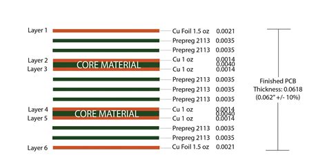
6-Layer Stackup
For more complex designs or high-speed applications, a 6-layer PCB stackup may be necessary. A typical 6-layer stackup includes:
| Layer | Description |
|---|---|
| Top | Signal layer |
| Inner 1 | Ground plane |
| Inner 2 | Signal layer |
| Inner 3 | Power plane |
| Inner 4 | Signal layer |
| Bottom | Signal layer |
This stackup provides additional signal layers for routing, while maintaining the benefits of dedicated ground and power planes. The signal layers can be arranged to minimize crosstalk and optimize signal integrity.
High-Layer-Count Stackups
For highly complex designs or high-density interconnect (HDI) PCBs, stackups with 8, 10, or more layers may be required. In these cases, the stackup design becomes more intricate, with multiple signal, ground, and power layers. High-layer-count stackups offer increased routing density and flexibility but come at a higher cost and manufacturing complexity.

Best Practices for PCB Stackup Design
To optimize your PCB stackup design, consider the following best practices:
- Define the layer requirements based on the circuit complexity, signal integrity, and power delivery needs.
- Use a symmetrical stackup whenever possible to minimize warpage and improve manufacturability.
- Maintain consistent dielectric thickness between layers to ensure controlled impedance and minimize signal distortion.
- Use a solid ground plane to provide a low-impedance return path and reduce EMI.
- Separate analog and digital signals to minimize crosstalk and interference.
- Place critical signals on inner layers to provide shielding and reduce external noise coupling.
- Use via shielding and stitching to minimize signal coupling and improve EMI performance.
- Collaborate with your PCB manufacturer to ensure that your stackup design is compatible with their fabrication capabilities and guidelines.
Frequently Asked Questions (FAQ)
- What is the minimum number of layers required for a PCB?
-
The minimum number of layers for a PCB is one, known as a single-layer PCB. However, most modern PCBs have at least two layers (double-layer PCBs) to accommodate more complex circuits and improve signal integrity.
-
How do I determine the number of layers needed for my PCB?
-
The number of layers needed for your PCB depends on factors such as circuit complexity, signal integrity requirements, power delivery needs, and routing density. Start by evaluating these factors and consulting with experienced PCB designers or manufacturers to determine the optimal layer count for your specific application.
-
What is the purpose of having dedicated ground and power planes in a PCB stackup?
-
Dedicated ground and power planes in a PCB stackup serve several purposes:
- They provide a low-impedance path for return currents, minimizing voltage drops and ensuring stable power delivery.
- They act as reference planes for the signal layers, reducing EMI and providing shielding.
- They help to maintain signal integrity by reducing crosstalk and providing a consistent reference for controlled impedance.
-
Can I mix different dielectric materials in the same PCB stackup?
-
While it is possible to mix different dielectric materials in the same PCB stackup, it is generally not recommended. Using different materials can lead to challenges in controlling impedance, ensuring consistent manufacturing, and maintaining reliability. It is best to use the same dielectric material throughout the stackup unless there are specific requirements that demand the use of multiple materials.
-
How does the PCB stackup design affect the manufacturing cost?
- The PCB stackup design has a significant impact on the manufacturing cost. Factors that influence the cost include:
- Number of layers: Higher layer counts generally result in higher manufacturing costs due to increased material usage and processing steps.
- Material selection: Some high-performance dielectric materials, such as Rogers laminates, are more expensive than standard FR-4.
- Dielectric thickness: Thinner dielectrics may require more precise manufacturing processes, leading to higher costs.
- Aspect ratio: High aspect ratio (thickness to diameter) vias or small via sizes can increase manufacturing complexity and cost.
- Impedance control: Tight impedance tolerances may require additional processing steps and more stringent quality control, resulting in higher costs.
Conclusion
Designing a PCB stackup is a critical aspect of PCB design that directly impacts the performance, reliability, and cost of the final product. By understanding the basics of PCB layers, considering signal integrity, power delivery, and EMI/EMC factors, and following best practices, you can create optimal PCB stackups for your projects.
Remember to collaborate with your PCB manufacturer and consider their capabilities and guidelines when designing your stackup. With careful planning and execution, you can ensure that your PCB stackup meets your design requirements and delivers the desired performance.
Leave a Reply