Introduction to PCB Vias
Printed Circuit Boards (PCBs) are essential components in modern electronics. They provide a reliable and efficient way to connect electronic components and create complex circuits. One crucial aspect of PCB design is the use of vias, which are small holes drilled through the PCB layers to establish electrical connections between different layers. In this article, we will explore the different types of PCB vias, their design considerations, and the various methods used for covering and protecting them.
Types of PCB Vias
Through-Hole Vias
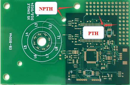
Through-hole vias are the most common type of vias used in PCB design. They are drilled through all layers of the PCB and are typically plated with a conductive material, such as copper, to ensure reliable electrical connections. Through-hole vias offer several advantages:
- Excellent mechanical strength and durability
- Easy to inspect and repair
- Suitable for high-power applications
However, through-hole vias also have some drawbacks:
- Require more space on the PCB compared to other via types
- Increase the overall thickness of the PCB
- Limit the routing density due to their larger size
Blind Vias
Blind vias are drilled from one side of the PCB and terminate at a specific inner layer without passing through the entire board. They offer several benefits over through-hole vias:
- Reduce the overall thickness of the PCB
- Allow for higher routing density
- Improve signal integrity by reducing the via length
However, blind vias also have some limitations:
- More expensive to manufacture compared to through-hole vias
- Require specialized equipment and processes
- Limited to connecting outer layers to inner layers
Buried Vias
Buried vias are located entirely within the inner layers of a PCB and do not extend to either surface of the board. They provide several advantages:
- Enable higher routing density on inner layers
- Improve signal integrity by reducing the via length
- Allow for more compact PCB designs
However, buried vias also have some drawbacks:
- Most expensive to manufacture among all via types
- Require specialized equipment and processes
- Difficult to inspect and repair
Micro Vias
Micro vias are small-diameter vias, typically less than 150 microns, used in high-density interconnect (HDI) PCB designs. They offer several benefits:
- Enable higher routing density and smaller component pitch
- Improve signal integrity by reducing the via length and inductance
- Allow for more compact PCB designs
However, micro vias also have some limitations:
- Require specialized manufacturing processes, such as laser drilling
- More expensive to manufacture compared to larger vias
- Limited to connecting outer layers to the first few inner layers

PCB Via Design Considerations
When designing PCB vias, several factors must be considered to ensure optimal performance, reliability, and manufacturability.
Via Size and Aspect Ratio
The size of a via is determined by its diameter and the thickness of the PCB. The aspect ratio, which is the ratio of the via depth to its diameter, is a critical factor in via design. A higher aspect ratio can lead to manufacturing challenges, such as difficulty in plating the via walls evenly. It is essential to follow the PCB manufacturer’s guidelines for via size and aspect ratio to ensure reliable and cost-effective production.
Via Placement and Spacing
Via placement and spacing are crucial for maintaining signal integrity and avoiding manufacturing issues. Vias should be placed as close to the components as possible to minimize the signal path length and reduce inductance. However, sufficient spacing must be maintained between vias and other features, such as traces and components, to prevent shorts and ensure proper insulation.
Via Pad Size and Annular Ring
The via pad is the copper area surrounding the via hole on the outer layers of the PCB. The annular ring is the minimum width of the copper pad around the via hole. Adequate via pad size and annular ring are essential for ensuring reliable electrical connections and mechanical strength. The PCB manufacturer’s design rules should be followed to determine the appropriate via pad size and annular ring for a given via size and PCB thickness.
Via Impedance Matching
In high-speed PCB designs, via impedance matching is critical for maintaining signal integrity and minimizing reflections. The impedance of a via depends on its geometry, the dielectric material surrounding it, and the frequency of the signal. To achieve impedance matching, techniques such as via stitching, back-drilling, and differential pair vias can be used.

PCB Via Covering and Protection
PCB vias must be properly covered and protected to ensure reliable operation and prevent damage from environmental factors such as moisture, dust, and debris.
Solder Mask
Solder mask is a thin, protective coating applied to the outer layers of a PCB. It covers the copper traces and vias, leaving only the exposed pads for component soldering. Solder mask helps to prevent shorts, protect the PCB from corrosion, and provide electrical insulation. When applying solder mask over vias, it is essential to ensure that the mask material flows evenly into the via holes and forms a reliable seal.
Via Filling
Via filling is the process of filling the via holes with a non-conductive material, such as epoxy or resin, to provide additional protection and improve the PCB’s mechanical strength. Via filling is particularly useful in applications where the PCB is subject to vibration, thermal stress, or high-pressure environments. Filled vias also help to prevent the entrapment of contaminants and moisture, which can lead to corrosion and reliability issues.
Via Capping
Via capping is a process where a thin layer of conductive material, typically copper or conductive paste, is applied over the via holes on the outer layers of the PCB. Via capping helps to improve the electrical and thermal conductivity of the vias, as well as provide additional protection against moisture and corrosion. Capped vias also offer a smooth, flat surface for component placement and soldering.

Frequently Asked Questions (FAQ)
- What is the difference between a through-hole via and a blind via?
-
A through-hole via passes through all layers of the PCB, while a blind via starts from one side of the PCB and terminates at a specific inner layer without passing through the entire board.
-
What is the purpose of via filling?
-
Via filling is used to provide additional protection and improve the mechanical strength of the PCB by filling the via holes with a non-conductive material, such as epoxy or resin.
-
Why is via impedance matching important in high-speed PCB designs?
-
Via impedance matching is critical in high-speed PCB designs to maintain signal integrity and minimize reflections. Mismatched via impedance can lead to signal distortion, crosstalk, and reduced performance.
-
What is the role of solder mask in PCB via protection?
-
Solder mask is a thin, protective coating applied to the outer layers of a PCB that covers the copper traces and vias, leaving only the exposed pads for component soldering. It helps to prevent shorts, protect the PCB from corrosion, and provide electrical insulation.
-
What are micro vias, and when are they used?
- Micro vias are small-diameter vias, typically less than 150 microns, used in high-density interconnect (HDI) PCB designs. They enable higher routing density, improve signal integrity, and allow for more compact PCB designs in applications with limited space or high component density.
Conclusion
PCB vias are essential components in modern electronics, providing reliable electrical connections between different layers of a PCB. Understanding the various types of vias, their design considerations, and the methods used for covering and protecting them is crucial for creating high-quality, reliable PCBs. By selecting the appropriate via type, following design guidelines, and implementing proper via covering and protection techniques, designers can ensure optimal performance and longevity of their PCB-based electronic devices.
As PCB technology continues to advance, new via technologies and manufacturing processes are emerging to meet the ever-increasing demands for higher density, faster speeds, and improved reliability. Keeping up with these advancements and working closely with experienced PCB manufacturers will be key to successful PCB design and production in the future.
| Via Type | Description | Advantages | Disadvantages |
|---|---|---|---|
| Through-Hole | Drilled through all PCB layers | – Excellent mechanical strength – Easy to inspect and repair – Suitable for high-power applications |
– Require more space – Increase PCB thickness – Limit routing density |
| Blind | Drilled from one side, terminate at inner layer | – Reduce PCB thickness – Allow higher routing density – Improve signal integrity |
– More expensive to manufacture – Require specialized equipment – Limited to connecting outer to inner layers |
| Buried | Located entirely within inner layers | – Enable higher routing density on inner layers – Improve signal integrity – Allow more compact designs |
– Most expensive to manufacture – Require specialized equipment – Difficult to inspect and repair |
| Micro | Small-diameter vias (< 150 µm) for HDI designs | – Enable higher routing density – Improve signal integrity – Allow more compact designs |
– Require specialized manufacturing – More expensive than larger vias – Limited to connecting outer to first few inner layers |
Leave a Reply