What is OSP PCB Finish and Why is it Used?
Organic Solderability Preservative (OSP) is a widely used surface finish for Printed Circuit Boards (PCBs). OSP is applied to the copper pads and traces on a PCB to prevent oxidation and maintain solderability during storage and assembly. Compared to other finishes like HASL, ENIG, and Immersion Silver, OSP offers several advantages:
- Lower cost
- Flatter surface (coplanarity)
- Easier inspection
- Thinner coating (does not affect fine pitch components)
- Environmentally friendly (lead-free and no hazardous chemicals)
The main component in OSP is benzimidazole, an organic compound that bonds to the copper surface and forms a protective layer 0.2-0.5 μm thick. This shields the copper from oxidation while allowing solder to bond during assembly.
OSP Application Process
The OSP coating is applied to PCBs through a multi-step process:
-
Cleaning: The bare PCB is cleaned to remove any contaminants or oxides from the copper surface. This is typically done by dipping the board in a mild acid.
-
Microetching: The clean copper surface is microetched to roughen it slightly. This increases the surface area for better adhesion of the OSP. A solution of hydrogen peroxide and sulfuric acid is commonly used.
-
Rinsing: The board is rinsed thoroughly with deionized water to remove any etchant residues.
-
OSP Application: The PCB is immersed in the liquid OSP solution, usually for 60-90 seconds. The benzimidazole bonds to the copper, forming a thin organic layer.
-
Drying: Hot air is used to dry the OSP-coated board and remove any moisture.
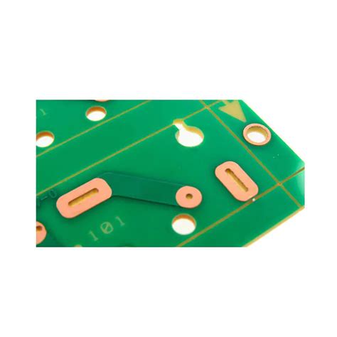
The resulting OSP surface has a distinctive bluish-purple color. This allows visual confirmation of coverage and aids in inspecting the PCB for any defects or contamination.
Common Problems with OSP PCB Finish
Despite its many benefits, OSP does have some drawbacks and potential issues that can impact PCB Assembly and reliability. The most common problems include:
1. Poor Wetting
One of the most frequently encountered issues with OSP finish is poor wetting during soldering. Possible causes include:
- Contamination of the OSP surface
- Degradation of the OSP coating over time
- Insufficient fluxing during assembly
- Incorrect reflow profile
If solder does not properly wet to the OSP-coated pads, it can result in open circuits, high resistance connections, or unreliable solder joints. X-ray inspection and microsectioning may be needed to detect and analyze poor wetting defects under BGAs and other hard-to-inspect components.
2. Chemical Attack
The benzimidazole in OSP is an organic compound that can react with certain chemicals. Exposure to strong acids, bases, oxidizers, or some solvents can degrade or strip away the OSP coating.
Common causes of chemical attack on OSP include:
- Overly aggressive or incompatible cleaning chemistries
- Flux residues from assembly
- Handling boards with bare hands (salts and oils on skin)
- Adhesives used to secure components
- Spills and fumes from other assembly processes
If the OSP is compromised by chemical attack, the underlying copper can corrode and cause solderability and reliability issues. Discoloration or smutting of the OSP surface may indicate chemical degradation has occurred.
3. Thickness Variation
For optimal performance, the OSP coating should be uniform in thickness across the PCB. If the OSP is too thin in some areas, it may not adequately protect the copper from oxidation. If it is too thick, it can impede soldering and affect solder joint geometry.
OSP thickness is affected by factors like:
- Immersion time in OSP bath
- OSP solution concentration
- Withdrawal speed from bath
- Microetch effectiveness
- Roughness of copper surface
Inconsistent OSP thickness is more likely on high-aspect ratio boards and those with very small pads or vias. Thickness variations can be difficult to detect visually but may be measured using XRF or other analytical techniques.
4. Shelf Life Limitations
Compared to metallic PCB finishes, OSP has a shorter shelf life before solderability degrades. The IPC J-STD-003 standard recommends a maximum storage time of 6 months for OSP-coated boards in sealed bags.
However, actual shelf life depends on many variables:
- Storage temperature and humidity
- Handling and packaging methods
- Atmospheric contaminants
- OSP formulation and thickness
Exceeding the rated shelf life increases the risk of solderability issues due to copper oxidation. Re-baking OSP PCBs before assembly can help restore solderability. Conducting wetting balance tests at different aging intervals is recommended to assess the impact of storage time on OSP performance.
5. Touchup and Rework Challenges
Removing and replacing components on OSP boards can be more difficult than with other finishes. The high heat of rework can burn off the OSP, exposing the copper to rapid oxidation. Fluxes and solder pastes may also interact with and degrade the surrounding OSP coating.
Some strategies to mitigate rework issues on OSP include:
- Using lower temperature, localized heat sources
- Applying liquid OSP or other protective coatings to reworked areas
- Minimizing time between component removal and replacement
- Thorough cleaning of flux residues after rework
In general, it is best to avoid rework on OSP boards whenever possible. If a high degree of rework is anticipated, a more durable finish like ENIG may be preferable.

Preventing and Troubleshooting OSP Problems
While OSP finish problems can adversely impact PCB assembly and reliability, most can be prevented or corrected by following best practices:
OSP Process Control
Consistent OSP quality starts with a well-controlled coating process. This includes:
- Using fresh, properly maintained OSP chemistry
- Monitoring and adjusting bath parameters (temperature, pH, concentration)
- Verifying adequate cleaning and microetching of copper surfaces
- Optimizing immersion time and withdrawal speed
- Routinely measuring OSP thickness
- Frequent visual and solderability inspections
Process data should be recorded and analyzed to identify trends and catch issues early. Many OSP defects are caused by deviations from the qualified process window.
Packaging and Handling
Proper packaging and handling of OSP coated boards is essential to preventing contamination, chemical attack, and oxidation. Recommendations include:
- Use ESD-safe materials that do not emit corrosive compounds
- Store boards in sealed moisture barrier bags with desiccant
- Avoid touching OSP surfaces with bare hands
- Wear gloves when handling and only grip boards by edges
- Do not stack OSP boards without protective interleaving
- Minimize exposure to high humidity and temperature extremes
Boards should be packaged immediately after OSP coating. Unsealed OSP PCBs can begin to oxidize in a matter of hours when exposed to air.
Design for OSP
Certain PCB Design choices can make OSP finishing more robust and less prone to problems. Guidelines include:
- Use larger pad sizes and avoid overly fine pitch when possible
- Specify wider trace widths and spaces
- Minimize number of copper layers and vias
- Avoid very thin laminate materials
- Provide soldermask dams between pads to constrain solder wicking
- Chamfer or round pad edges to eliminate OSP “weak spots”
Designers should follow IPC-4761 Design Guide for Protection of PCBs and work closely with fabricators to ensure OSP compatibility.
Assembly Process Optimization
To achieve good soldering and long-term reliability with OSP, the assembly process must be optimized. Key considerations include:
- Selecting OSP-compatible solder paste and flux
- Printing solder paste with adequate volume and registration
- Controlling reflow profile to prevent OSP damage
- Cleaning flux residues promptly after reflow
- Baking boards before assembly if solderability is suspect
The table below shows recommended reflow parameters for OSP with SAC305 solder paste:
| Profile Parameter | Acceptable Range |
|---|---|
| Ramp Rate | 1-3°C/sec |
| Preheat Temp | 150-200°C |
| Preheat Time | 60-180 sec |
| Peak Temp | 235-255°C |
| Time Above 217°C | 60-150 sec |
Reflow settings may need to be adjusted based on specific paste and equipment. Profiling and wetting balance testing should be conducted to optimize the process.
Inspection and Testing
Vigilant inspection and testing are critical to identifying OSP problems before and after assembly. Common methods include:
- Visual examination of OSP surface for color, texture, and contamination
- Solderability testing per J-STD-002 (wetting balance, dip & look, etc.)
- Optical/SEM inspection of solder joints for wetting and geometry
- Cross-sectioning of joints to check intermetallic formation
- Electrical Testing for opens and shorts
- Accelerated aging and environmental testing of assembled boards
Inspection data should be used to troubleshoot OSP issues and drive continuous process improvement. Catching problems early can prevent costly scrap and rework.

FAQ
1. What is the shelf life of OSP coated PCBs?
The shelf life of OSP PCBs depends on several factors, including storage conditions, handling, and OSP quality. In general, IPC standards recommend a maximum storage time of 6 months in sealed packaging. However, actual shelf life may be shorter or longer depending on the specific circumstances. Accelerated aging tests can help determine the useful life of OSP boards in a given environment.
2. Can you rework OSP PCBs?
Yes, OSP PCBs can be reworked, but it is more challenging than with other finishes. The high heat of rework can degrade the OSP coating and cause rapid oxidation of exposed copper. To minimize damage, use localized heating methods and apply liquid OSP or other coatings to protect reworked areas. Thorough cleaning of flux residues is also important. If extensive rework is expected, consider using a more rework-friendly finish like ENIG.
3. How do you test the solderability of OSP PCBs?
There are several methods to assess the solderability of OSP PCBs:
- Wetting Balance Test (J-STD-002): Measures the wetting force of molten solder on OSP surface
- Dip & Look Test: Dips board in solder bath and visually examines extent of wetting
- Edge Dip Test: Dips board edge in solder and measures % wetted area
- Rotary Dip Test: Clamps board to a rotating drum and dips in solder, measuring % coverage
SACMA recommends the wetting balance test as the most quantitative and informative method. Solderability should be tested at multiple points in the PCB life cycle to ensure consistency.
4. What causes poor wetting on OSP PCBs?
Poor wetting on OSP boards can have several root causes:
- Contamination of OSP surface by dirt, oils, salts, etc.
- Oxidation or chemical degradation of OSP coating due to prolonged storage or exposure
- Thin or inconsistent OSP thickness
- Insufficient fluxing during soldering
- Improper reflow profile (ramp rate, peak temp, TAL)
To troubleshoot wetting issues, start by examining the OSP surface for signs of contamination or degradation. Then review the OSP coating process and storage/handling conditions. Finally, optimize the assembly process, including paste/flux selection, printing, and reflow.
5. How does OSP compare to other PCB finishes?
OSP has some advantages and disadvantages compared to other common PCB finishes:
-
HASL (Hot Air Solder Leveling): OSP is flatter, cheaper, and uses less solder, but HASL has better durability and shelf life.
-
ENIG (Electroless Nickel Immersion Gold): ENIG is more expensive than OSP but offers superior corrosion resistance, shelf life, and reworkability. It is commonly used for gold finger contacts.
-
Immersion Silver: Like OSP, immersion silver is a thin, flat, solderable finish. Silver also has good shelf life and leach resistance. However, it is prone to tarnishing and is incompatible with some ROHS-compliant solders.
The best finish choice depends on the specific PCB design, environment, and assembly process. In general, OSP provides a good mix of low cost, solderability, and flatness for many applications.

Conclusion
OSP is a popular and cost-effective PCB finish that can enable high-yield assembly when properly applied and controlled. However, it is not without its challenges, including shelf life limitations, chemical sensitivity, and rework difficulties.
By understanding the potential failure modes of OSP and implementing best practices in design, processing, and handling, it is possible to avoid or mitigate many common OSP problems. This includes:
- Robust process controls and monitoring
- Proper packaging and storage
- Design optimization for OSP
- Compatible assembly materials and parameters
- Thorough inspection and testing
No PCB finish is perfect for every application. But by weighing the tradeoffs and proactively managing risks, OSP can provide reliable solderability and performance in a wide range of products. As with any complex manufacturing process, communication and collaboration between designers, fabricators, and assemblers is key to OSP success.
Leave a Reply