Understanding the DRC-Kicad-issue
Kicad is a powerful open-source electronic design automation (EDA) software that helps users design printed circuit boards (PCBs). One of its essential features is the Design Rule Check (DRC), which ensures that the PCB design adheres to a set of predefined rules and constraints. However, users may encounter issues when working with ground planes in Kicad, leading to DRC errors. In this article, we will explore the common problems associated with DRC and Kicad ground planes and provide solutions to overcome them.
What is a Ground Plane?
A ground plane is a large copper area on a PCB that provides a low-impedance return path for electrical currents. It helps to reduce electromagnetic interference (EMI), improves signal integrity, and provides a stable reference voltage for the circuit. In Kicad, users can create ground planes using the copper pour feature, which automatically fills the designated areas with copper.
Common DRC Errors Related to Ground Planes
When running DRC on a PCB design with ground planes, users may encounter various errors. Some of the most common issues include:
-
Clearance violations: This error occurs when the distance between the ground plane and other components or traces is less than the specified clearance value.
-
Copper pour not connected: This error indicates that the ground plane is not properly connected to the desired net, usually the GND net.
-
Thermal relief issues: Thermal relief pads help to dissipate heat during soldering. If the thermal relief settings are not configured correctly, DRC may flag errors related to insufficient or excessive thermal relief.
-
Acid traps: Acid traps are small, isolated copper areas that can cause issues during PCB fabrication. DRC may report acid trap errors if the ground plane contains such isolated areas.
Resolving DRC Errors Related to Ground Planes
Adjusting Clearance Settings
To resolve clearance violations, users need to adjust the clearance settings in the Kicad PCB editor. Follow these steps:
- Open the PCB editor and navigate to the “Design Rules” dialog.
- Select the “Clearance” tab and modify the “Copper to Copper” clearance value to ensure sufficient spacing between the ground plane and other components or traces.
- Click “OK” to apply the changes and re-run the DRC to verify that the clearance violations have been resolved.
Ensuring Proper Net Connection
If the DRC reports that the copper pour is not connected to the desired net, follow these steps to resolve the issue:
- Select the copper pour zone in the PCB editor.
- Right-click on the zone and choose “Properties.”
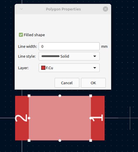
- In the “Properties” dialog, ensure that the “Net” field is set to the correct net (usually GND).
- Click “OK” to apply the changes and re-run the DRC.
Configuring Thermal Relief Settings
To address thermal relief issues, users need to configure the thermal relief settings in the Kicad PCB editor. Follow these steps:
- Select the copper pour zone in the PCB editor.
- Right-click on the zone and choose “Properties.”
- In the “Properties” dialog, navigate to the “Thermal Relief” tab.
- Adjust the “Spoke Width,” “Spoke Angle,” and “Thermal Gap” settings according to your PCB fabrication requirements.
- Click “OK” to apply the changes and re-run the DRC.
Eliminating Acid Traps
To remove acid traps from the ground plane, users can employ the following techniques:
- Increase the “Minimum Width” setting for the copper pour zone to avoid creating small, isolated copper areas.
- Use the “Keep Out” or “Restrict” features to exclude specific areas from the copper pour, preventing the formation of acid traps.
- Manually edit the copper pour zone to remove any isolated copper areas that DRC identifies as acid traps.

Best Practices for Working with Ground Planes in Kicad
To minimize DRC errors and ensure optimal PCB design when working with ground planes in Kicad, consider the following best practices:
- Plan your PCB layout carefully, taking into account the placement of components, traces, and ground planes.
- Use appropriate clearance settings to maintain sufficient spacing between the ground plane and other elements.
- Ensure that the ground plane is properly connected to the desired net (usually GND) to establish a low-impedance return path.
- Configure thermal relief settings according to your PCB fabrication requirements to facilitate soldering and heat dissipation.
- Avoid creating small, isolated copper areas (acid traps) in the ground plane, as they can cause issues during PCB fabrication.
- Regularly run DRC checks throughout the design process to identify and resolve any issues related to ground planes.
| Issue | Solution |
|---|---|
| Clearance violations | Adjust clearance settings in the “Design Rules” dialog |
| Copper pour not connected | Ensure the copper pour zone is set to the correct net (usually GND) |
| Thermal relief issues | Configure thermal relief settings in the copper pour zone properties |
| Acid traps | Increase minimum width, use “Keep Out” or “Restrict” features, manually edit zone |

Frequently Asked Questions (FAQ)
-
Q: What is the purpose of a ground plane in a PCB design?
A: A ground plane provides a low-impedance return path for electrical currents, reduces electromagnetic interference (EMI), improves signal integrity, and provides a stable reference voltage for the circuit. -
Q: How can I create a ground plane in Kicad?
A: In Kicad, you can create a ground plane using the copper pour feature. Select the desired area, right-click, and choose “Fill Zone.” Configure the properties, such as the net connection and thermal relief settings, and click “OK” to create the ground plane. -
Q: What should I do if DRC reports clearance violations related to the ground plane?
A: To resolve clearance violations, open the “Design Rules” dialog in the PCB editor, navigate to the “Clearance” tab, and adjust the “Copper to Copper” clearance value to ensure sufficient spacing between the ground plane and other components or traces. -
Q: How can I ensure that the ground plane is properly connected to the desired net?
A: Select the copper pour zone, right-click, and choose “Properties.” In the “Properties” dialog, verify that the “Net” field is set to the correct net (usually GND). Click “OK” to apply the changes. -
Q: What are acid traps, and how can I avoid them in my ground plane?
A: Acid traps are small, isolated copper areas that can cause issues during PCB fabrication. To avoid them, increase the “Minimum Width” setting for the copper pour zone, use the “Keep Out” or “Restrict” features to exclude specific areas, and manually edit the zone to remove any isolated copper areas identified by DRC.
By understanding the common issues related to DRC and Kicad ground planes, following best practices, and implementing the solutions outlined in this article, users can effectively resolve DRC errors and ensure optimal PCB design. Regular DRC checks and attention to detail throughout the design process will help minimize issues and streamline the PCB fabrication process.

Leave a Reply