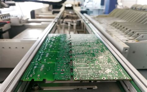
What is Reflow Soldering?
Reflow soldering is a method of soldering electronic components to a PCB using solder paste, which is a mixture of tiny solder particles suspended in flux. The process involves applying solder paste to the PCB pads, placing components onto the paste, and then heating the entire assembly in a controlled manner to melt the solder particles and form a strong electrical and mechanical bond between the components and the PCB.
Advantages of Reflow Soldering
- High efficiency: Reflow soldering allows for the simultaneous soldering of multiple components, greatly reducing assembly time compared to manual soldering methods.
- Consistency: The controlled heating process ensures consistent and reliable solder joints across the entire PCB.
- Precision: Solder paste can be applied with high precision, enabling the soldering of small and closely spaced components.
- Automation: Reflow soldering is easily automated, making it suitable for high-volume production runs.
Equipment Required for Reflow Soldering
To perform reflow soldering effectively, you will need the following equipment:
- Solder paste: A mixture of tiny solder particles and flux, available in various alloy compositions and particle sizes.
- Stencil: A thin metal sheet with openings that match the PCB pad layout, used to apply solder paste accurately.
- Squeegee: A tool used to spread solder paste evenly across the stencil and onto the PCB pads.
- Pick-and-Place machine (optional): An automated system for placing components onto the PCB with high speed and precision.
- Reflow oven: A specialized oven that heats the PCB Assembly through a controlled temperature profile to melt the solder and form connections.

The Reflow Soldering Process
The reflow soldering process consists of several key steps:
1. PCB Preparation
Before applying solder paste, ensure that the PCB is clean and free from contaminants. If necessary, clean the PCB with isopropyl alcohol or a specialized PCB cleaner. Inspect the PCB for any defects or irregularities in the pad layout.
2. Solder Paste Application
Place the stencil over the PCB, aligning it with the pads. Apply solder paste to the stencil and use the squeegee to spread the paste evenly across the stencil, filling the openings. Remove the stencil carefully, leaving precise deposits of solder paste on the PCB pads.
3. Component Placement
Place the components onto the solder paste deposits on the PCB. This can be done manually using tweezers for small-scale projects or with a pick-and-place machine for larger production runs. Ensure that the components are correctly oriented and seated firmly in the solder paste.
4. Reflow Soldering
Place the populated PCB into the reflow oven. The oven will heat the assembly through a predetermined temperature profile, typically consisting of four stages:
a. Preheat: The PCB is gradually heated to activate the flux and remove any moisture.
b. Soak: The temperature is maintained to allow the components and PCB to reach a uniform temperature.
c. Reflow: The temperature is quickly raised above the melting point of the solder, causing the solder particles to melt and form connections between the components and PCB pads.
d. Cooling: The PCB is cooled gradually to solidify the solder joints and prevent thermal shock.
The specific temperature profile will depend on the type of solder paste used and the requirements of the components being soldered.
5. Inspection and Rework
After the reflow soldering process is complete, visually inspect the PCB for any defects, such as bridging (unintended connections between pads), insufficient solder, or misaligned components. If necessary, perform rework using a soldering iron or hot air rework station to correct any issues.

Reflow Soldering Temperature Profile
The temperature profile is a critical aspect of the reflow soldering process, as it determines the quality and reliability of the solder joints. A typical reflow soldering temperature profile consists of four stages:
| Stage | Temperature Range | Duration |
|---|---|---|
| Preheat | 25°C to 150°C | 30-90 seconds |
| Soak | 150°C to 180°C | 60-120 seconds |
| Reflow | 220°C to 250°C | 30-60 seconds |
| Cooling | 250°C to 25°C | 30-90 seconds |
It is essential to follow the recommended temperature profile for the specific solder paste and components used in your project. Deviating from the optimal profile can lead to issues such as poor wetting, cold solder joints, or damage to the components.

Solder Paste Selection
Selecting the appropriate solder paste is crucial for achieving high-quality solder joints. Solder paste is available in various alloy compositions, such as tin-lead (SnPb) or lead-free (e.g., SAC305), and different particle sizes. The choice of solder paste depends on factors such as the component size, PCB pad geometry, and the desired melting temperature.
When choosing a solder paste, consider the following:
- Alloy composition: Lead-free solder pastes, such as SAC305 (96.5% tin, 3% silver, 0.5% copper), are becoming increasingly popular due to environmental and health concerns. However, tin-lead solder pastes, such as Sn63Pb37 (63% tin, 37% lead), are still used in some applications.
- Particle size: Solder paste is classified by its particle size, with Type 3 (25-45 microns) and Type 4 (20-38 microns) being the most common. Smaller particle sizes are suitable for fine-pitch components and smaller PCB pads.
- Flux type: Solder paste contains flux, which helps to remove oxides and promote wetting during the soldering process. Flux types include rosin-based (RMA), water-soluble (OA), and no-clean (NC). Choose the flux type based on the cleaning requirements and the desired level of residue on the PCB post-soldering.
Stencil Design Considerations
The stencil is a critical tool in the reflow soldering process, as it determines the accuracy and consistency of solder paste deposition. When designing a stencil, consider the following factors:
- Stencil thickness: The stencil thickness should be selected based on the PCB pad size and the desired solder paste volume. Typical stencil thicknesses range from 0.1 mm to 0.2 mm (4 to 8 mils).
- Aperture size: The aperture size should be slightly larger than the PCB pad to allow for proper solder paste release. A common guideline is to add 10% to the pad size for the aperture dimensions.
- Aperture shape: The aperture shape can affect the solder paste release and the resulting solder joint. Common shapes include square, circular, and home plate (a combination of square and circular).
- Stencil material: Stainless steel is the most common material for stencils due to its durability and precision. However, polyimide or nickel-plated stencils may be used for specific applications.
Troubleshooting Common Reflow Soldering Issues
Despite careful planning and execution, issues can still arise during the reflow soldering process. Some common problems and their potential solutions include:
- Bridging: Solder bridges can form between adjacent pads due to excessive solder paste, incorrect stencil design, or improper component placement. To prevent bridging, ensure that the stencil apertures are appropriately sized, the solder paste volume is controlled, and the components are correctly placed.
- Insufficient solder: Insufficient solder can result in weak or open connections. This issue may be caused by inadequate solder paste deposition, incorrect stencil design, or poor wetting during the reflow process. To resolve this, verify the stencil aperture sizes, ensure proper solder paste application, and optimize the reflow temperature profile.
- Tombstoning: Tombstoning occurs when a component stands up on one end due to uneven heating or surface tension imbalances. To prevent tombstoning, ensure that the PCB pads are symmetrical, the reflow temperature profile is optimized, and the component placement is accurate.
- Solder balls: Solder balls are small spheres of solder that can form on the PCB surface due to excessive solder paste or incorrect reflow temperature profiles. To minimize solder ball formation, control the solder paste volume, use a nitrogen atmosphere in the reflow oven, and optimize the temperature profile.
By understanding these common issues and their causes, you can take preventive measures and troubleshoot problems more effectively during the reflow soldering process.
Frequently Asked Questions (FAQ)
- What is the difference between reflow soldering and wave soldering?
-
Reflow soldering is used for surface mount components and involves applying solder paste to the PCB pads, placing components, and heating the assembly to melt the solder. Wave soldering, on the other hand, is used for through-hole components and involves passing the PCB over a molten solder wave to form connections.
-
Can I reflow solder without a stencil?
-
While it is possible to apply solder paste manually without a stencil, using a stencil is highly recommended for achieving consistent and precise solder paste deposition. Manual application can lead to inconsistencies and defects in the solder joints.
-
How do I choose the right solder paste for my project?
-
When selecting a solder paste, consider factors such as the alloy composition (lead-free or tin-lead), particle size (Type 3 or Type 4), and flux type (rosin-based, water-soluble, or no-clean). Choose the paste that best suits your components, PCB pad sizes, and cleaning requirements.
-
What is the purpose of flux in solder paste?
-
Flux is a chemical agent that helps to remove oxides from the metal surfaces being soldered, promoting better wetting and stronger solder joint formation. Flux also helps to prevent oxidation during the reflow soldering process.
-
Can I reflow solder a PCB multiple times?
- While it is possible to reflow solder a PCB multiple times, it is not recommended unless absolutely necessary. Each reflow cycle subjects the components and PCB to thermal stress, which can lead to degradation and reduced reliability. If rework is required, use localized heating methods, such as a soldering iron or hot air rework station, to minimize the impact on the entire assembly.
By understanding the fundamentals of reflow soldering, selecting the appropriate equipment and materials, and following best practices, you can achieve high-quality solder joints and reliable electronic assemblies. Reflow soldering is a versatile and efficient process that is essential for modern electronics manufacturing, and mastering this technique can open up new possibilities for your projects and designs.
Leave a Reply