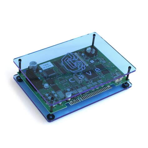
Understanding the Requirements for PCB Enclosure Design
Before starting the design process, it is crucial to understand the specific requirements for your PCB enclosure. These requirements may include:
- Environmental factors (e.g., temperature, humidity, dust, and moisture)
- Mechanical factors (e.g., impact, vibration, and shock)
- Electrical factors (e.g., electromagnetic interference (EMI) and electrostatic discharge (ESD))
- Aesthetic and ergonomic considerations
- Manufacturing and assembly constraints
- Regulatory and industry standards
By clearly defining these requirements, you can ensure that your enclosure design meets the necessary criteria for protecting and housing your PCBA.
Choosing the Right Material for Your PCB Enclosure
The choice of material for your PCB enclosure depends on various factors, such as the environmental conditions, mechanical requirements, and cost constraints. Some common materials used for PCB enclosures include:
| Material | Advantages | Disadvantages |
|---|---|---|
| Plastic (e.g., ABS, polycarbonate) | – Lightweight – Cost-effective – Easy to mold and customize |
– Limited heat dissipation – Lower strength compared to metals |
| Metal (e.g., aluminum, steel) | – Excellent heat dissipation – High strength and durability – Good EMI shielding |
– Higher cost – Heavier than plastic – More difficult to customize |
| Composite materials (e.g., carbon fiber) | – High strength-to-weight ratio – Good thermal and electrical properties |
– Expensive – Complex manufacturing process |
Consider the specific requirements of your application and choose a material that provides the best balance of properties and cost.

Designing for Thermal Management
Thermal management is a critical aspect of PCB enclosure design, as excessive heat can lead to component failure and reduced product lifespan. When designing your enclosure, consider the following thermal management techniques:
-
Passive cooling: Use heat sinks, thermal pads, and thermal interface materials to conduct heat away from components and dissipate it through the enclosure.
-
Active cooling: Incorporate fans or other active cooling solutions to force air through the enclosure and remove heat from critical components.
-
Ventilation: Design air vents and openings in the enclosure to allow for natural convection and air circulation.
-
Thermal simulations: Use thermal simulation software to analyze the heat distribution within the enclosure and optimize the design for effective thermal management.

Incorporating Electromagnetic Interference (EMI) Shielding
EMI can cause interference with other electronic devices and lead to product malfunctions. To minimize EMI, consider incorporating the following shielding techniques in your PCB enclosure design:
-
Conductive coatings: Apply conductive coatings, such as nickel or copper, to the interior of the enclosure to create a Faraday cage and attenuate EMI.
-
Gaskets and seals: Use conductive gaskets and seals around doors, panels, and other openings to maintain the integrity of the EMI shielding.
-
Shielding materials: Incorporate shielding materials, such as metal foils or conductive plastics, into the enclosure design to block EMI.
-
Grounding: Ensure proper grounding of the enclosure and components to minimize EMI and improve overall system performance.

Designing for Assembly and Manufacturing
To ensure efficient and cost-effective production, consider the following assembly and manufacturing aspects when designing your PCB enclosure:
-
Simplicity: Keep the design as simple as possible to minimize the number of parts and streamline the assembly process.
-
Modularity: Design the enclosure in modular sections to facilitate easier assembly and maintenance.
-
Fastening methods: Choose appropriate fastening methods, such as snap-fits, screws, or adhesives, based on the enclosure material and assembly requirements.
-
Tolerances: Specify appropriate tolerances for the enclosure dimensions to ensure proper fit and functionality of the PCBA and other components.
-
Manufacturing processes: Consider the capabilities and limitations of the chosen manufacturing processes, such as injection molding, die casting, or CNC machining, when designing the enclosure.
Prototyping and Testing
Before finalizing your PCB enclosure design, it is essential to create prototypes and conduct thorough testing to validate the design and identify any potential issues. Consider the following prototyping and testing methods:
-
3D printing: Use 3D printing technology to create rapid prototypes of your enclosure design for visual and functional evaluation.
-
CNC machining: Fabricate prototypes using CNC machining for more accurate and durable representations of the final product.
-
Environmental testing: Subject the prototypes to various environmental conditions, such as temperature extremes, humidity, and vibration, to ensure the enclosure provides adequate protection for the PCBA.
-
EMI testing: Conduct EMI testing to verify that the enclosure effectively shields the PCBA from electromagnetic interference.
-
User testing: Engage potential users to evaluate the ergonomics, aesthetics, and overall functionality of the enclosure design.
Based on the results of the prototyping and testing phase, make any necessary adjustments to the design before proceeding with mass production.
Frequently Asked Questions (FAQ)
-
What is the importance of designing a proper enclosure for a PCBA?
A well-designed enclosure protects the PCBA from environmental factors, physical damage, and electromagnetic interference, ensuring optimal performance and longevity of the electronic product. -
How do I choose the right material for my PCB enclosure?
The choice of material depends on factors such as environmental conditions, mechanical requirements, and cost constraints. Consider the specific needs of your application and select a material that provides the best balance of properties and cost. -
What are some common thermal management techniques used in PCB enclosure design?
Common thermal management techniques include passive cooling (heat sinks, thermal pads), active cooling (fans), ventilation, and thermal simulations to optimize the design for effective heat dissipation. -
How can I minimize electromagnetic interference (EMI) in my PCB enclosure design?
To minimize EMI, consider incorporating conductive coatings, gaskets and seals, shielding materials, and proper grounding in your enclosure design. -
Why is prototyping and testing important in the PCB enclosure design process?
Prototyping and testing allow you to validate the design, identify potential issues, and make necessary adjustments before proceeding with mass production, ultimately saving time and resources in the long run.
Conclusion
Designing an enclosure for a PCBA is a critical aspect of electronic product development that requires careful consideration of various factors, including environmental conditions, mechanical requirements, thermal management, EMI shielding, and manufacturing constraints. By understanding these requirements, choosing the right materials, and incorporating appropriate design techniques, you can create a robust and effective enclosure that protects and enhances the performance of your PCBA. Remember to prototype and test your design thoroughly to ensure it meets all the necessary criteria before proceeding with mass production.
Leave a Reply