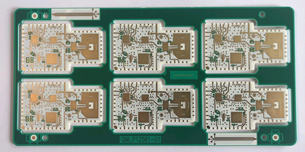
Introduction to High Frequency PCBs
Printed circuit boards (PCBs) that operate at high frequencies, typically above 1 GHz, are known as high frequency PCBs. They are used in applications like radars, satellites, 5G networks, WiFi routers, mobile phones, etc. The main characteristics of high frequency PCBs are:
- Tight tolerances
- Controlled impedance
- Low loss materials
- Short trace lengths
- Proper grounding and shielding
These features are critical for the PCB to function properly at high frequencies where wavelengths get shorter and signal integrity becomes very important. Let’s look at some of these aspects in more detail:
Tight Tolerances

At high frequencies, small variations in trace widths, dielectric thickness etc. can significantly impact the performance. So high frequency PCBs require very tight tolerances, often down to +/- 0.005″ for trace width and thickness. The manufacturers need advanced processes and tight process controls to achieve such precision repeatedly.
Controlled Impedance
The traces on high frequency PCBs must maintain a specific characteristic impedance, usually 50 or 75 ohms. This prevents signal reflections due to impedance mismatches. The trace width, height above the reference plane and dielectric material determines the impedance. Maintaining tight tolerances on all three is critical.
Low Loss Materials
Dielectric materials used must have low dissipation factor to minimize signal loss. Popular low loss materials include PTFE, ceramic filled PTFE, hydrocarbon ceramics, etc. Some exotic materials like polyphenylene ether (PPE) blends are used in extremely high frequency applications.
Short Trace Lengths
Long traces tend to act like antennas and radiate energy. At high frequencies, a quarter wavelength trace can act as an efficient antenna. To avoid unwanted radiation and susceptibility, trace lengths must be kept as short as possible.
Proper Grounding/Shielding
A continuous reference plane is essential for controlling impedance. Multiple layer boards with solid ground planes are used. Sensitive circuits may need shielding enclosures to contain electromagnetic interference (EMI). Connectors must have 360 degree shielding.
Key Requirements from a High Frequency PCB Manufacturer
Based on the above discussion, here are some key requirements when selecting a high frequency PCB manufacturer:
- Use of advanced materials like PTFE composites, hydrocarbons, ceramic filled laminates etc.
- Capability to fabricate multilayer boards, typically 4-16 layers.
- Fine line/space capability down to at least 6/6 mil lines/spaces.
- Tight process controls to meet tolerance requirements.
- Plating control for uniform copper thickness.
- Smooth copper foils that don’t distort controlled impedance lines.
- Capability to fabricate blind/buried vias for routing signals between layers.
- Impedance control techniques – which can be simulated pre-manufacturing.
- Testing and inspection methods to verify impedance, signal integrity etc.
Choosing the Right High Frequency PCB Manufacturer
Here are some tips on how to select the right high frequency PCB manufacturer:
- Make sure they have expertise in high frequency designs and not just regular PCBs.
- Review examples of prior high frequency PCB work. Evaluate complexity and frequency range.
- Ask about the materials, stackups, tolerances etc. they can support.
- Evaluate their process capabilities based on needs of your specific design.
- Discuss impedance control methods and any pre-production simulation/modeling.
- Understand lead time, testing procedures, qualification process etc.
- Check credentials like quality certifications such as ISO, IPC certifications etc.
- Get references from prior customers with similar high frequency needs.
High Frequency PCB Design Tips
Here are some design tips to optimize your high frequency PCB layout:
- Keep traces short, use stubless designs with angular routing.
- Use a ground fill on inner layers for continuous reference plane.
- Keep out regions around connectors for uninterrupted ground return paths.
- Use vias to stitch top and bottom ground planes. Avoid splits in ground planes.
- Carefully match component pads, trace widths to maintain impedance.
- Use landing patterns for decoupling capacitors. Keep them close to ICs.
- Add geometric shapes for shielding sensitive signals or circuits.
- Simulate and tweak design before manufacturing to avoid costly re-spins.
Frequently Asked Questions

Q1. What are some examples of high frequency PCB applications?
Some common examples include 5G equipment, WiFi routers, automotive radars, defense electronics, satellite communication, etc. Generally anything above 1 GHz is considered a high frequency application.
Q2. What board materials are used for high frequency PCBs?
PTFE composites like Rogers RO4000, hydrocarbon ceramics like Arlon 25N and ceramic filled PTFE materials are commonly used. Some manufacturers also use exotic materials like polyphenylene ether (PPE) blends for extreme high frequencies.
Q3. How is impedance controlled in high frequency PCBs?
Trace width, thickness and material dielectric constant determine characteristic impedance. Precise fabrication and micro-etching techniques are used to maintain tight width/thickness tolerances. Dielectric constant of material is well controlled.
Q4. Why are shorter traces preferred in high frequency designs?
At high frequencies traces behave like antennas and radiate energy. A quarter wavelength trace makes an efficient antenna. Shorter traces reduce radiation losses and EMI issues.
Q5. What special analyses are done for high frequency PCBs?
Simulation of impedance, resonant frequency, signal loss, EMI, power integrity, thermal analysis and vibration/shock analysis are typically performed. These minimize the risk of re-spins later.

Leave a Reply